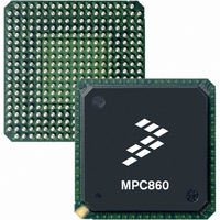
MPC855TCVR50D4 Freescale Semiconductor, MPC855TCVR50D4 Datasheet - Page 85

MPC855TCVR50D4
Manufacturer Part Number
MPC855TCVR50D4
Description
IC MPU POWERQUICC 50MHZ 357PBGA
Manufacturer
Freescale Semiconductor
Datasheets
1.MPC855TVR50D4.pdf
(15 pages)
2.MPC8555ECVTALF.pdf
(88 pages)
3.MPC855TCVR50D4.pdf
(80 pages)
Specifications of MPC855TCVR50D4
Processor Type
MPC8xx PowerQUICC 32-Bit
Speed
50MHz
Voltage
3.3V
Mounting Type
Surface Mount
Package / Case
357-PBGA
Processor Series
MPC8xx
Core
MPC8xx
Data Bus Width
32 bit
Maximum Clock Frequency
50 MHz
Operating Supply Voltage
2.5 V, 3.3 V
Maximum Operating Temperature
+ 95 C
Mounting Style
SMD/SMT
Minimum Operating Temperature
- 40 C
Family Name
MPC8xx
Device Core
PowerQUICC
Device Core Size
32b
Frequency (max)
50MHz
Instruction Set Architecture
RISC
Supply Voltage 1 (typ)
2.5/3.3V
Operating Supply Voltage (max)
3.465/3.6V
Operating Supply Voltage (min)
2/3.135V
Operating Temp Range
-40C to 95C
Operating Temperature Classification
Industrial
Mounting
Surface Mount
Pin Count
357
Package Type
BGA
Lead Free Status / RoHS Status
Lead free / RoHS Compliant
Features
-
Lead Free Status / Rohs Status
Lead free / RoHS Compliant
Available stocks
Company
Part Number
Manufacturer
Quantity
Price
Company:
Part Number:
MPC855TCVR50D4
Manufacturer:
FREESCAL
Quantity:
246
Company:
Part Number:
MPC855TCVR50D4
Manufacturer:
Freescale Semiconductor
Quantity:
10 000
Company:
Part Number:
MPC855TCVR50D4R2
Manufacturer:
Freescale Semiconductor
Quantity:
10 000
18 Document Revision History
Table 51
Freescale Semiconductor
Rev. No.
4.2
4.1
3.2
3.1
4
3
2
1
0
MPC8555E PowerQUICC™ III Integrated Communications Processor Hardware Specification, Rev. 4.2
provides a revision history for this hardware specification.
12/2006
11/2006
10/2005
1/2008
7/2007
8/2005
8/2005
6/2005
6/2005
Date
Added “Note: Rise/Fall Time on CPM Input Pins” and following note text to
Timing
Inserted
Updated
Updated back page information.
Updated
Replaced
Added footnote 2 about junction temperature in
Added max. power values for 1000 MHz core frequency in
Removed
Modified note to t
Changed t
Added note 3 to t
Modified note 3 in
Added note 3 to t
Modified values for t
Changed Input Signals: LAD[0:31]/LDP[0:3] in
Modified note for signal CLK_OUT in
PCI1_CLK and PCI2_CLK changed from I/O to I in
Added column for Encryption Acceleration in
Modified max. power values in
Modified notes for signals TSEC1_TXD[3:0], TSEC2_TXD[3:0], TRIG_OUT/READY, MSRCID4,
CLK_OUT, and MDVAL in
Previous revision’s history listed incorrect cross references. Table 2 is now correctly listed as
Table 27
Added note 2 in
Modified min and max values for t
Changed LV
Modified footnote 4 and changed typical power for the 1000 MHz core frequency
Corrected symbols for body rows 9–15, effectively changing them from a high state to a low state
in
Initial release.
Table
Specifications.”
31.
Figure
Section 2.1.2, “Power Sequencing.”
Section 2.1.2, “Power Sequencing.”
and Table 38 is now listed as
Section 17.8, “JTAG Configuration Signals.”
Figure
LBKHOZ1
Table 51. Document Revision History
dd
to OV
3, ““Maximum AC Waveforms on PCI interface for 3.3-V Signaling.”
Table
3, “Maximum AC Waveforms on PCI Interface for 3.3-V Signaling.”
LBKHOV1
LBKLOV1
LBKSKEW
Table 30
and t
LBKHKT
dd
7.
for the supply voltage Ethernet management interface in
LBKHOV2
in
in
Table
from 8 to 9 in
, t
and
Table
Table
LBKLOV1
Table
Table
43.
values
DDKHMP
31.
30.
Substantive Change(s)
, t
4.
Table
31.
LBKLOV2
Table
inTable
Table
in
43.
Table
31.
Table
30.
, t
Figure
Table
30.
LBKLOV3
14.
52.
Table
4.
21.
, t
43.
LBKLOZ1
Table
4.
, and t
Document Revision History
LBKLOZ2
Section 10.2, “CPM AC
Table
in
inTable
Table
27.
4.
31.
85


