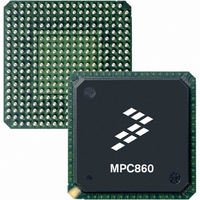
MPC855TCVR50D4 Freescale Semiconductor, MPC855TCVR50D4 Datasheet - Page 5

MPC855TCVR50D4
Manufacturer Part Number
MPC855TCVR50D4
Description
IC MPU POWERQUICC 50MHZ 357PBGA
Manufacturer
Freescale Semiconductor
Datasheets
1.MPC855TVR50D4.pdf
(15 pages)
2.MPC8555ECVTALF.pdf
(88 pages)
3.MPC855TCVR50D4.pdf
(80 pages)
Specifications of MPC855TCVR50D4
Processor Type
MPC8xx PowerQUICC 32-Bit
Speed
50MHz
Voltage
3.3V
Mounting Type
Surface Mount
Package / Case
357-PBGA
Processor Series
MPC8xx
Core
MPC8xx
Data Bus Width
32 bit
Maximum Clock Frequency
50 MHz
Operating Supply Voltage
2.5 V, 3.3 V
Maximum Operating Temperature
+ 95 C
Mounting Style
SMD/SMT
Minimum Operating Temperature
- 40 C
Family Name
MPC8xx
Device Core
PowerQUICC
Device Core Size
32b
Frequency (max)
50MHz
Instruction Set Architecture
RISC
Supply Voltage 1 (typ)
2.5/3.3V
Operating Supply Voltage (max)
3.465/3.6V
Operating Supply Voltage (min)
2/3.135V
Operating Temp Range
-40C to 95C
Operating Temperature Classification
Industrial
Mounting
Surface Mount
Pin Count
357
Package Type
BGA
Lead Free Status / RoHS Status
Lead free / RoHS Compliant
Features
-
Lead Free Status / Rohs Status
Lead free / RoHS Compliant
Available stocks
Company
Part Number
Manufacturer
Quantity
Price
Company:
Part Number:
MPC855TCVR50D4
Manufacturer:
FREESCAL
Quantity:
246
Company:
Part Number:
MPC855TCVR50D4
Manufacturer:
Freescale Semiconductor
Quantity:
10 000
Company:
Part Number:
MPC855TCVR50D4R2
Manufacturer:
Freescale Semiconductor
Quantity:
10 000
Freescale Semiconductor
•
•
•
— Can be partitioned into 128-Kbyte L2 cache plus 128-Kbyte SRAM
— Full ECC support on 64-bit boundary in both cache and SRAM modes
— SRAM operation supports relocation and is byte-accessible
— Cache mode supports instruction caching, data caching, or both
— External masters can force data to be allocated into the cache through programmed memory
— Eight-way set-associative cache organization (1024 sets of 32-byte cache lines)
— Supports locking the entire cache or selected lines
— Global locking and flash clearing done through writes to L2 configuration registers
— Instruction and data locks can be flash cleared separately
— Read and write buffering for internal bus accesses
Address translation and mapping unit (ATMU)
— Eight local access windows define mapping within local 32-bit address space
— Inbound and outbound ATMUs map to larger external address spaces
DDR memory controller
— Programmable timing supporting first generation DDR SDRAM
— 64-bit data interface, up to MHz data rate
— Four banks of memory supported, each up to 1 Gbyte
— DRAM chip configurations from 64 Mbits to 1 Gbit with x8/x16 data ports
— Full ECC support
— Page mode support (up to 16 simultaneous open pages)
— Contiguous or discontiguous memory mapping
— Sleep mode support for self refresh DDR SDRAM
— Supports auto refreshing
— On-the-fly power management using CKE signal
— Registered DIMM support
— Fast memory access via JTAG port
— 2.5-V SSTL2 compatible I/O
Programmable interrupt controller (PIC)
— Programming model is compliant with the OpenPIC architecture
— Supports 16 programmable interrupt and processor task priority levels
— Supports 12 discrete external interrupts
— Supports 4 message interrupts with 32-bit messages
MPC8555E PowerQUICC™ III Integrated Communications Processor Hardware Specification, Rev. 4.2
ranges or special transaction types (stashing).
– Individual line locks set and cleared through Book E instructions or by externally mastered
– Three inbound windows plus a configuration window on PCI
– Four inbound windows
– Four outbound windows plus default translation for PCI
transactions
Overview
5


