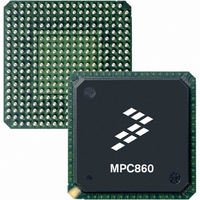
MPC855TCVR50D4 Freescale Semiconductor, MPC855TCVR50D4 Datasheet - Page 64

MPC855TCVR50D4
Manufacturer Part Number
MPC855TCVR50D4
Description
IC MPU POWERQUICC 50MHZ 357PBGA
Manufacturer
Freescale Semiconductor
Datasheets
1.MPC855TVR50D4.pdf
(15 pages)
2.MPC8555ECVTALF.pdf
(88 pages)
3.MPC855TCVR50D4.pdf
(80 pages)
Specifications of MPC855TCVR50D4
Processor Type
MPC8xx PowerQUICC 32-Bit
Speed
50MHz
Voltage
3.3V
Mounting Type
Surface Mount
Package / Case
357-PBGA
Processor Series
MPC8xx
Core
MPC8xx
Data Bus Width
32 bit
Maximum Clock Frequency
50 MHz
Operating Supply Voltage
2.5 V, 3.3 V
Maximum Operating Temperature
+ 95 C
Mounting Style
SMD/SMT
Minimum Operating Temperature
- 40 C
Family Name
MPC8xx
Device Core
PowerQUICC
Device Core Size
32b
Frequency (max)
50MHz
Instruction Set Architecture
RISC
Supply Voltage 1 (typ)
2.5/3.3V
Operating Supply Voltage (max)
3.465/3.6V
Operating Supply Voltage (min)
2/3.135V
Operating Temp Range
-40C to 95C
Operating Temperature Classification
Industrial
Mounting
Surface Mount
Pin Count
357
Package Type
BGA
Lead Free Status / RoHS Status
Lead free / RoHS Compliant
Features
-
Lead Free Status / Rohs Status
Lead free / RoHS Compliant
Available stocks
Company
Part Number
Manufacturer
Quantity
Price
Company:
Part Number:
MPC855TCVR50D4
Manufacturer:
FREESCAL
Quantity:
246
Company:
Part Number:
MPC855TCVR50D4
Manufacturer:
Freescale Semiconductor
Quantity:
10 000
Company:
Part Number:
MPC855TCVR50D4R2
Manufacturer:
Freescale Semiconductor
Quantity:
10 000
Package and Pin Listings
64
GND
GV
LV
MV
No Connects
OV
RESERVED
SENSEVDD
SENSEVSS
V
PA[8:31]
DD
DD
DD
DD
REF
MPC8555E PowerQUICC™ III Integrated Communications Processor Hardware Specification, Rev. 4.2
Signal
A12, A17, B3, B14, B20, B26, B27, C2, C4, C11,C17,
C19, C22, C27, D8, E3, E12, E24, F11, F18, F23, G9,
V10, V26, W5, W18, W23, Y8, Y16, AA6, AA13, AB4,
AB11, AB19, AC6, AC9, AD3, AD8, AD17, AF2, AF4,
F19, F25, G13, G18, G20, G23, G28, H19, H24, J12,
D1, E4, H3, K4, K10, L7, M5, N3, P22, R19, R25, T2,
T7, U5, U20, U26, V8, W4, W13, W19, W21, Y7, Y23,
M13, M15, M17, N14, N16, P13, P15, P17, R12, R14,
J7, J8, K8, K7, K6, K3, K2, K1, L1, L2, L3, L4, L5, L8,
M14, M16, M22, M27, N2, N13, N15, N17, P12, P14,
C28, D16, D19, D21, D24, D28, E17, E22, F12, F15,
J24, K5, K9, K18, K23, K28, L6, L20, L25, M4, M12,
A14, A20, A25, A26, A27, A28, B17, B22, B28, C12,
AE25, AE26, AE27, AF24, AF25, H1, H2, J1, J2, J3,
G12, G25, H4, H12, H14, H17, H20, H22, H27, J19,
J17, J22, J27, K15, K20, K25, L13, L23, L28, M25,
V25, W24, W25, W9, Y24, Y25, Y5, Y6, Y9, AH26,
J4, J5, J6, M1, N1, N10, N11, N4, N5, N7, N8, N9,
T12, T14, T16, U6, U13, U15, U16, U17, U21, V7,
P16, P23, R13, R15, R17, R20, R26, T3, T8, T10,
P10, P8, P9, R10, R11, T24, T25, U24, U25, V24,
AA5, AA12, AA16, AA20, AB7, AB9, AB26, AC5,
AC11, AC17, AD4, AE1, AE8, AE10, AE15, AF7,
AA24, AA25, AA3, AA4, AA7 AA8, AB24, AB25,
AC24, AC25, AD23, AD24, AD25, AE23, AE24,
Table 43. MPC8555E Pinout Listing (continued)
AH28, AG28, AH1, AG1, AH2, B1, B2, A2, A3
L9, L10, L11, M10, M9, M8, M7, M6, M3, M2
AF10, AF13, AF15, AF27, AG3, AG7
R16, T13, T15, T17, U12, U14
Package Pin Number
C1, T11, U11, AF1
AF12, AG27, AH4
A4, C5, E7, H10
N21
N27
K12
L12
CPM
Power for DDR
Voltage Signal;
other Standard
Power for Core
Power for Core
Ethernet, and
Three-Speed
(2.5 V, 3.3 V)
Ethernet I/O
PCI, 10/100
Reference
Reference
DRAM I/O
Pin Type
Voltage;
Voltage
(2.5 V)
(3.3 V)
(1.2 V)
(1.2 V)
DDR
—
—
—
—
I/0
Freescale Semiconductor
Supply
MV
Power
GV
OV
OV
LV
V
V
—
—
—
—
DD
DD
DD
REF
DD
DD
DD
Notes
16
15
13
13
—
—
—
—
—
—
—


