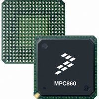
MC68MH360VR33L Freescale Semiconductor, MC68MH360VR33L Datasheet - Page 21

MC68MH360VR33L
Manufacturer Part Number
MC68MH360VR33L
Description
IC MPU QUICC 33MHZ 357-PBGA
Manufacturer
Freescale Semiconductor
Specifications of MC68MH360VR33L
Processor Type
M683xx 32-Bit
Speed
33MHz
Voltage
5V
Mounting Type
Surface Mount
Package / Case
357-PBGA
Family Name
M68000
Device Core
ColdFire
Device Core Size
32b
Frequency (max)
33MHz
Instruction Set Architecture
RISC
Supply Voltage 1 (typ)
5V
Operating Supply Voltage (max)
5.25V
Operating Supply Voltage (min)
4.75V
Operating Temp Range
0C to 70C
Operating Temperature Classification
Commercial
Mounting
Surface Mount
Pin Count
357
Package Type
BGA
Lead Free Status / RoHS Status
Lead free / RoHS Compliant
Features
-
Lead Free Status / Rohs Status
Compliant
Available stocks
Company
Part Number
Manufacturer
Quantity
Price
Company:
Part Number:
MC68MH360VR33L
Manufacturer:
Freescale Semiconductor
Quantity:
10 000
Company:
Part Number:
MC68MH360VR33LR2
Manufacturer:
Freescale Semiconductor
Quantity:
10 000
Freescale Semiconductor, Inc.
1.5.1 Synchronization
Independent receive and transmit clocks and frame synchronization signals control the data
transfer. In NMSI operation, synchronization occurs only once to initiate a transfer using
the CD (receive) and CTS (transmit) signals in pulse mode. If any noise corrupts either
signal, the QMC will be out of synchronization until the whole protocol is restarted.
In contrast, the more robust SI performs a synchronization on each frame, limiting the
damage from noise error on the clock or synchronization lines. Noisy channels can be
restarted individually without interrupting other channels. For more details about possible
errors in the TDM interface, see Section 1.8, “SI RAM Errors.”
1.5.2 Loopback Mode
The loopback from a transmitter to a receiver is implemented on a per channel basis for
every logical channel. A common transmit and receive clock as well as a common frame
synchronization pulse must be provided for loopback mode to work. The loopback is done
on a fixed time slot, meaning that if one logical channel transmits on time slot 17, the
loopback occurs through time slot 17 also, whether it is same logical channel or not that
receives the incoming data. The reason for this restriction is that no buffering is performed
after a channel is processed by the transmitter, or before it reaches the receiver.
Previously reserved, bit 15 of each entry in the SI-RAM is now the loopback bit controlling
the loopback for the corresponding time slot. It is important to have each individual time
slot as an entry in the SI-RAM for proper loopback on each individual channel.
1.5.3 Echo Mode
The SI can be programmed to echo incoming data. In this mode, the complete TDM link is
retransmitted from the incoming L1RXDx to the L1TXDx pin on a bit-by-bit basis. The
receiver section of the selected SCC can operate normally and also receive the incoming bit
stream. This is also known as global echo mode on the whole link. Individual time slot echo
is not possible with QMC without software intervention.
1.5.4 Inverted Signals
For each SCC, the DPLL can be used to invert the bitstream of the transmitter before the
signal reaches the pin. This is not a bit-order inversion, but a logical level inversion. The
DPLL can also invert the incoming data before it is forwarded to the receiver section. A
logical inversion on a per channel basis is not possible in the QMC without external
hardware. To invert a specific channel, the SI can be programmed to send a strobe signal at
the channel’s corresponding time slot, assuming the SCC is operating in QMC mode. This
strobe can then be connected to an external XOR gate to perform the inversion.
Chapter 1. Overview
For More Information On This Product,
Go to: www.freescale.com


