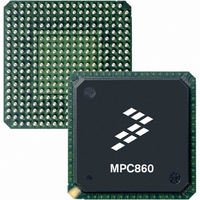
MC68MH360VR33L Freescale Semiconductor, MC68MH360VR33L Datasheet - Page 93

MC68MH360VR33L
Manufacturer Part Number
MC68MH360VR33L
Description
IC MPU QUICC 33MHZ 357-PBGA
Manufacturer
Freescale Semiconductor
Specifications of MC68MH360VR33L
Processor Type
M683xx 32-Bit
Speed
33MHz
Voltage
5V
Mounting Type
Surface Mount
Package / Case
357-PBGA
Family Name
M68000
Device Core
ColdFire
Device Core Size
32b
Frequency (max)
33MHz
Instruction Set Architecture
RISC
Supply Voltage 1 (typ)
5V
Operating Supply Voltage (max)
5.25V
Operating Supply Voltage (min)
4.75V
Operating Temp Range
0C to 70C
Operating Temperature Classification
Commercial
Mounting
Surface Mount
Pin Count
357
Package Type
BGA
Lead Free Status / RoHS Status
Lead free / RoHS Compliant
Features
-
Lead Free Status / Rohs Status
Compliant
Available stocks
Company
Part Number
Manufacturer
Quantity
Price
Company:
Part Number:
MC68MH360VR33L
Manufacturer:
Freescale Semiconductor
Quantity:
10 000
Company:
Part Number:
MC68MH360VR33LR2
Manufacturer:
Freescale Semiconductor
Quantity:
10 000
Step 5: Configure port C for TDMa and/or TDMb signals L1ST1, 2, 3, and/or 4;
L1TSYNCx and/or L1RSYNCx. For more information on port C, see page 7-365 of the
MC68360 User’s Manual and page 16-465 of the MPC860 User’s Manual.
The following setting enables L1RSYNCx, L1TSYNCx, and all L1STx strobes. Note that
if common clocking is used, selected by the CRTx bit in the SI MODE register, only
L1RSYNCx is required. Note that the L1STx functions are repeated on Port B and should
only be configured on one port.
Step 6: Write the values to the SI RAM locations that will route the time slots required. For
more information on SI RAM programming, see page 7-72 of the MC68360 User’s Manual
and page 16-106 of the MPC860 User’s Manual.
The following example configures every byte to be transferred to SCC1; note that the final
entry in both the Tx and Rx tables has the LST bit set. Also, this example for TDMa
assumes that SIGMR[RDM] is set to 0b10 (32 entries for Rx and Tx). If n is the last entry,
the following applies:
PCPAR = 0x0F0F;
PCDIR = 0x000F;
SIRAM[0] = 0x0042;
SIRAM[1] = 0x0042;
SIRAM[n-1] = 0x0043;
SIRAM[32] = 0x0042;
SIRAM[33] = 0x0042;
SIRAM[34] = 0x0042;
SIRAM[32+n] = 0x0043;
On the MH360, the SI RAM is mapped in a continuous 256-
byte block from REGB + 700->7FF. On the 860MH, it is
mapped to a 512-byte block from C00->DFF. Also on the
860MH, the SI RAM has 16-bit entries aligned to 32-bit
boundaries; therefore, only half of the actual address space is
valid (there are 256 valid bytes).
Freescale Semiconductor, Inc.
For More Information On This Product,
Go to: www.freescale.com
Chapter 6. QMC Initialization
/* init port C pin assignment register */
/* init port C data direction register */
/* init 1st receive element */
/* init 2nd receive element */
/* init nth receive element */
/* init 1st xmit element */
/* init 2nd xmit element */
/* init 3rd xmit element */
/* init nth xmit element */
NOTE


