DS21FF44 Maxim Integrated Products, DS21FF44 Datasheet - Page 32
DS21FF44
Manufacturer Part Number
DS21FF44
Description
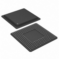
IC FRAMER E1 4X4 16CH 300-BGA
Manufacturer
Maxim Integrated Products
Datasheet
1.DS21FT44N.pdf
(117 pages)
Specifications of DS21FF44
Controller Type
E1 Framer
Interface
Parallel/Serial
Voltage - Supply
2.97 V ~ 3.63 V
Current - Supply
300mA
Operating Temperature
0°C ~ 70°C
Mounting Type
Surface Mount
Package / Case
300-BGA
Lead Free Status / RoHS Status
Contains lead / RoHS non-compliant
Available stocks
Company
Part Number
Manufacturer
Quantity
Price


DS21FT44/DS21FF44
9. PARALLEL PORT
The DS21Q44 is controlled by either a nonmultiplexed (MUX = 0) or a multiplexed (MUX = 1) bus by
an external microcontroller or microprocessor. The DS21Q44 can operate with either Intel or Motorola
bus timing configurations. If the BTS pin is connected low, Intel timing will be selected; if connected
high, Motorola timing will be selected. All Motorola bus signals are listed in parenthesis (). See the
timing diagrams in the A.C. Electrical Characteristics in Section 23 for more details.
10.
CONTROL, ID, AND TEST REGISTERS
The operation of each framer within the DS21Q44 is configured by a set of 10 control registers.
Typically, the control registers are only accessed when the system is first powered up. Once a channel in
the DS21Q44 has been initialized, the control registers will only need to be accessed when there is a
change in the system configuration. There are two Receive Control Register (RCR1 and RCR2), two
Transmit Control Registers (TCR1 and TCR2), and six Common Control Registers (CCR1 to CCR6).
Each of the ten registers are described in this section.
There is a device Identification Register (IDR) at address 0Fh. The MSB of this read-only register is fixed
to a one indicating that the DS21Q44 is present. The T1 pin-for-pin compatible version of the DS21Q44
is the DS21Q42 and it also has an ID register at address 0Fh and the user can read the MSB to determine
which chip is present since in the DS21Q42 the MSB will be set to a 0 and in the DS21Q44 it will be set
to a one. The lower 4 bits of the IDR are used to display the die revision of the chip.
Power-Up Sequence
The DS21Q44 does not automatically clear its register space on power-up. After the supplies are stable,
each of the four framer’s register space should be configured for operation by writing to all of the internal
registers. This includes setting the Test and all unused registers to 00Hex.
This can be accomplished using a two-pass approach on each framer within the DS21Q44.
1) Clear framer’s register space by writing 00H to the addresses 00H through 0BFH.
2) Program required registers to achieve desired operating mode.
NOTE:
When emulating the DS21Q43 feature set (FMS = 1), the full address space (00H through 0BFH) must be
initialized. DS21Q43 emulation require address pin A7 to be used. FMS is connected to ground for the
DS21FF44/DS21FT44.
Finally, after the TSYSCLK and RSYSCLK inputs are stable, the ESR bit should be toggled from a zero
to a one (this step can be skipped if the elastic stores are disabled).
32 of 117
Related parts for DS21FF44
Image
Part Number
Description
Manufacturer
Datasheet
Request
R

Part Number:
Description:
MAX7528KCWPMaxim Integrated Products [CMOS Dual 8-Bit Buffered Multiplying DACs]
Manufacturer:
Maxim Integrated Products
Datasheet:
Part Number:
Description:
Single +5V, fully integrated, 1.25Gbps laser diode driver.
Manufacturer:
Maxim Integrated Products
Datasheet:
Part Number:
Description:
Single +5V, fully integrated, 155Mbps laser diode driver.
Manufacturer:
Maxim Integrated Products
Datasheet:
Part Number:
Description:
VRD11/VRD10, K8 Rev F 2/3/4-Phase PWM Controllers with Integrated Dual MOSFET Drivers
Manufacturer:
Maxim Integrated Products
Datasheet:
Part Number:
Description:
Highly Integrated Level 2 SMBus Battery Chargers
Manufacturer:
Maxim Integrated Products
Datasheet:
Part Number:
Description:
Current Monitor and Accumulator with Integrated Sense Resistor; ; Temperature Range: -40°C to +85°C
Manufacturer:
Maxim Integrated Products
Part Number:
Description:
TSSOP 14/A�/RS-485 Transceivers with Integrated 100O/120O Termination Resis
Manufacturer:
Maxim Integrated Products
Part Number:
Description:
TSSOP 14/A�/RS-485 Transceivers with Integrated 100O/120O Termination Resis
Manufacturer:
Maxim Integrated Products
Part Number:
Description:
QFN 16/A�/AC-DC and DC-DC Peak-Current-Mode Converters with Integrated Step
Manufacturer:
Maxim Integrated Products
Part Number:
Description:
TDFN/A/65V, 1A, 600KHZ, SYNCHRONOUS STEP-DOWN REGULATOR WITH INTEGRATED SWI
Manufacturer:
Maxim Integrated Products
Part Number:
Description:
Integrated Temperature Controller f
Manufacturer:
Maxim Integrated Products
Part Number:
Description:
SOT23-6/I�/45MHz to 650MHz, Integrated IF VCOs with Differential Output
Manufacturer:
Maxim Integrated Products
Part Number:
Description:
SOT23-6/I�/45MHz to 650MHz, Integrated IF VCOs with Differential Output
Manufacturer:
Maxim Integrated Products
Part Number:
Description:
EVALUATION KIT/2.4GHZ TO 2.5GHZ 802.11G/B RF TRANSCEIVER WITH INTEGRATED PA
Manufacturer:
Maxim Integrated Products
Part Number:
Description:
QFN/E/DUAL PCIE/SATA HIGH SPEED SWITCH WITH INTEGRATED BIAS RESISTOR
Manufacturer:
Maxim Integrated Products
Datasheet: