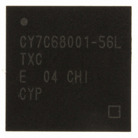
CY7C68001-56LTXC Cypress Semiconductor Corp, CY7C68001-56LTXC Datasheet - Page 43

CY7C68001-56LTXC
Manufacturer Part Number
CY7C68001-56LTXC
Description
IC USB EZ-USB SX2 HS 56VQFN
Manufacturer
Cypress Semiconductor Corp
Series
CY7Cr
Type
USBr
Specifications of CY7C68001-56LTXC
Protocol
USB 2.0
Voltage - Supply
3 V ~ 3.6 V
Mounting Type
Surface Mount
Package / Case
56-VQFN Exposed Pad, 56-HVQFN, 56-SQFN, 56-DHVQFN
Lead Free Status / RoHS Status
Lead free / RoHS Compliant
Number Of Drivers/receivers
-
Lead Free Status / Rohs Status
Lead free / RoHS Compliant
Other names
428-2932
Available stocks
Company
Part Number
Manufacturer
Quantity
Price
Part Number:
CY7C68001-56LTXC
Manufacturer:
CYPRESS/赛普拉斯
Quantity:
20 000
In burst read mode when the SLRD is asserted, the data is in a driven state and is the previous data. Once SLRD is asserted,
the data from the FIFO is output on the data bus (when SLOE is also in an asserted state) and the FIFO pointer is incremented.
Basically the data is fetched at the time of the read.
11.6.4
The above sequence diagram shows the timing relation between various signals while performing a write to the FIFO in
asynchronous mode. The diagram shows a single write followed by burst write of 3 bytes and committing the 4-bytes-short packet
using the PKTEND pin.
In this burst write mode once SLWR is deasserted, the data is written to the FIFO and the FIFO pointer is incremented. Asserting
the SLWR causes the data to be written to the FIFO and the FIFO pointer to be incremented to point to the next byte in the FIFO.
The FIFO pointer is post incremented.
In the above diagram once the four bytes are written to the FIFO and the SLWR is de-asserted, the short 4-byte packet can be
committed to the host using the PKTEND pinl. The external device should be designed so as to not have SLWR and PKTEND
pulsed at the same time. It should be designed so as to assert the PKTEND pin after the SLWR is deasserted and met the
minimum deasserted pulse width. The FIFOADDR lines should be held constant during the PKTEND pin assertion.
Document #: 38-08013 Rev. *B
FLAGS
FIFOADR
• At t = 0 the FIFO address is set making sure that it meets the setup time of t
• SLWR and SLCS is asserted at the same time. The SLWR must meet the minimum active pulse of t
• Data is then written to the data bus t
• De-asserting the SLWR causes the data on the data bus to be written to the FIFO and the FIFO pointer incremented. The flag
SLWR/
SLCS
SLCS
DATA
PKTEND
deactive pulse width of t
internal logic basically ANDs these two signal to determine a valid condition. Hence these signals can be tied together.
is also updated after t
Sequence Diagram of a Single and Burst Asynchronous Write
t=0
t
SFA
t
Figure 11-20. Slave FIFO Asynchronous Write Sequence and Timing Diagram
WRpwl
t
SFD
XFLG
WRpwh
t
N
FDH
t
WRpwh
from the deasserting edge of SLWR.
t
FAH
t
XFLG
. If SLCS is used then, SLCS must be in an asserted state when SLWR is also asserted. The
SFD
before the deasserting edge of the SLWR to meet the data setup time.
t
SFA
t
WRpwl
t
SFD
t
N+1
FDH
t
WRpwh
t
WRpwl
t
SFD
t
N+2
FDH
t
WRpwh
SFA.
t
WRpwl
t
SFD
t
N+3
t
FDH
WRpwh
WRpwl
t
PEpwl
[8]
CY7C68001
and minimum
t
XFLG
t
PEpwh
t
FAH
Page 43 of 50


