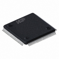
SAA7115HL/V1,518 NXP Semiconductors, SAA7115HL/V1,518 Datasheet - Page 191

SAA7115HL/V1,518
Manufacturer Part Number
SAA7115HL/V1,518
Description
IC DIGITAL VIDEO DECODER 100LQFP
Manufacturer
NXP Semiconductors
Type
Video Decoderr
Specifications of SAA7115HL/V1,518
Package / Case
100-LQFP
Applications
Set-Top Boxes
Mounting Type
Surface Mount
Mounting Style
SMD/SMT
Lead Free Status / RoHS Status
Lead free / RoHS Compliant
Voltage - Supply, Analog
-
Voltage - Supply, Digital
-
Lead Free Status / RoHS Status
Lead free / RoHS Compliant, Lead free / RoHS Compliant
Other names
935270666518
SAA7115HLBE-T
SAA7115HLBE-T
SAA7115HLBE-T
SAA7115HLBE-T
Available stocks
Company
Part Number
Manufacturer
Quantity
Price
Company:
Part Number:
SAA7115HL/V1,518
Manufacturer:
Sigma Designs Inc
Quantity:
10 000
- Current page: 191 of 548
- Download datasheet (6Mb)
Philips Semiconductors
reliable operation of an 166- MHz (T
system.
Table 12-17. Critical 166-MHz SDRAM parameters
For a 183 MHz operation, SDRAM devices must meet
the critical specifications listed in
reliable operation of an 183- MHz (T
ory system.
Table 12-18. Critical 183-MHz SDRAM parameters
These values leave virtually no margin for the critical tim-
ing parameters in a high-speed system and assume a to-
tal worst case delay from 0.6 ns to 0.4 ns (From 143 MHz
to 183 MHz operating frequency the trace layout must be
improved to reduce trace delay as well as skew) and a
T
The maximum operating frequency is usually computed
with the following equation:
Where T
MM_CLK1, and T
in
trace delay and trace skew.
Max. output delay
Min. output hold time
Max. input setup time
Max. input hold time
Max. output delay
Min. output hold time
Max. input setup time
Max. input hold time
SU
T
Section 1.9.7.10 on page
cycle
for PNX1300 of 0 ns.
≥
CS
Timing Parameter
Timing Parameter
t
AC
is the skew between MM_CLK0 and
+
T
SU
board
the input data setup time as defined
+
t
t
t
t
t
t
t
t
AC
OH
IS
IH
AC
OH
IS
IH
T
CS
1-19, and T
+
T
Table 12-18
SU
cycle
cycle
.
= 6 ns) memory
= 5.4 ns) mem-
board
5.5 ns
2.0 ns
1.5 ns
1.0 ns
5.0 ns
2.0 ns
1.5 ns
1.0 ns
Value
Value
to ensure
includes
12.16.1 Main AC Parameter requirements
The PNX1300 SDRAM interface was designed to sup-
port a wide range of SDRAM vendors.
scribes some of the minimum SDRAM AC requirements
for PNX1300 to operate correctly. The symbols or names
are not really standardized and may differ from one ven-
dor to another one. The table is not meant to be exhaus-
tive and shows only the main parameters. Parameters
are expressed in clock cycles rather than ns.
Table 12-19. Minimum AC Parameters
12.17 EXAMPLE BLOCK DIAGRAMS
The following figures illustrate some of the memory con-
figurations that can be built with PNX1300. For all them
the signals used as bank addresses, are interchange-
able (i.e. it does not matter which of the two signals is
connected to Bank 1 or Bank 0 of the SDRAM device).
12.17.1 Block Diagrams for a 32-bit interface
The following sections present examples of possible
connections with 16-, 64-, 128- and 256 Mbit SDRAMs.
MM_CONFIG.BW must be set to ‘0’ (refer to bw,
Section
12.17.1.1 16-Mbit Devices or Less
These devices allow small memory configurations to be
built. They are described in more details in the TM-1000
and TM-1100 Databooks.
PRELIMINARY SPECIFICATION
ACTIVE command period
ACTIVE to PRECHARGE command
PRECHARGE command period
ACTIVE Bank A to ACTIVE bank B
ACTIVE to READ or WRITE command
WRITE recovery time
12.6.1).
Description
SDRAM Memory System
Table
t
t
t
t
t
t
Symbol Clocks
RC
RAS
RP
RRD
RCD
WR
12-19, de-
10
12-9
7
3
3
3
2
Related parts for SAA7115HL/V1,518
Image
Part Number
Description
Manufacturer
Datasheet
Request
R

Part Number:
Description:
IC ADV DGTL VIDEO DECODR 100LQFP
Manufacturer:
NXP Semiconductors
Datasheet:

Part Number:
Description:
Video ICs ADV DGTL VIDEO DECODR
Manufacturer:
NXP Semiconductors
Datasheet:
Part Number:
Description:
Ntsc/pal/secam 9-bit Video Decoder
Manufacturer:
NXP Semiconductors
Datasheet:
Part Number:
Description:
NXP Semiconductors designed the LPC2420/2460 microcontroller around a 16-bit/32-bitARM7TDMI-S CPU core with real-time debug interfaces that include both JTAG andembedded trace
Manufacturer:
NXP Semiconductors
Datasheet:

Part Number:
Description:
NXP Semiconductors designed the LPC2458 microcontroller around a 16-bit/32-bitARM7TDMI-S CPU core with real-time debug interfaces that include both JTAG andembedded trace
Manufacturer:
NXP Semiconductors
Datasheet:
Part Number:
Description:
NXP Semiconductors designed the LPC2468 microcontroller around a 16-bit/32-bitARM7TDMI-S CPU core with real-time debug interfaces that include both JTAG andembedded trace
Manufacturer:
NXP Semiconductors
Datasheet:
Part Number:
Description:
NXP Semiconductors designed the LPC2470 microcontroller, powered by theARM7TDMI-S core, to be a highly integrated microcontroller for a wide range ofapplications that require advanced communications and high quality graphic displays
Manufacturer:
NXP Semiconductors
Datasheet:
Part Number:
Description:
NXP Semiconductors designed the LPC2478 microcontroller, powered by theARM7TDMI-S core, to be a highly integrated microcontroller for a wide range ofapplications that require advanced communications and high quality graphic displays
Manufacturer:
NXP Semiconductors
Datasheet:
Part Number:
Description:
The Philips Semiconductors XA (eXtended Architecture) family of 16-bit single-chip microcontrollers is powerful enough to easily handle the requirements of high performance embedded applications, yet inexpensive enough to compete in the market for hi
Manufacturer:
NXP Semiconductors
Datasheet:
Part Number:
Description:
The XA-S3 device is a member of Philips Semiconductors? XA(eXtended Architecture) family of high performance 16-bitsingle-chip microcontrollers
Manufacturer:
NXP Semiconductors
Datasheet:

Part Number:
Description:
The NXP BlueStreak LH75401/LH75411 family consists of two low-cost 16/32-bit System-on-Chip (SoC) devices
Manufacturer:
NXP Semiconductors
Datasheet:

Part Number:
Description:
The NXP LPC3130/3131 combine an 180 MHz ARM926EJ-S CPU core, high-speed USB2
Manufacturer:
NXP Semiconductors
Datasheet:

Part Number:
Description:
The NXP LPC3141 combine a 270 MHz ARM926EJ-S CPU core, High-speed USB 2
Manufacturer:
NXP Semiconductors


