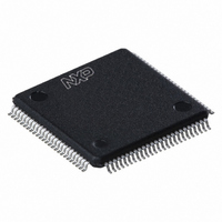
SAA7115HL/V1,518 NXP Semiconductors, SAA7115HL/V1,518 Datasheet - Page 207

SAA7115HL/V1,518
Manufacturer Part Number
SAA7115HL/V1,518
Description
IC DIGITAL VIDEO DECODER 100LQFP
Manufacturer
NXP Semiconductors
Type
Video Decoderr
Specifications of SAA7115HL/V1,518
Package / Case
100-LQFP
Applications
Set-Top Boxes
Mounting Type
Surface Mount
Mounting Style
SMD/SMT
Lead Free Status / RoHS Status
Lead free / RoHS Compliant
Voltage - Supply, Analog
-
Voltage - Supply, Digital
-
Lead Free Status / RoHS Status
Lead free / RoHS Compliant, Lead free / RoHS Compliant
Other names
935270666518
SAA7115HLBE-T
SAA7115HLBE-T
SAA7115HLBE-T
SAA7115HLBE-T
Available stocks
Company
Part Number
Manufacturer
Quantity
Price
Company:
Part Number:
SAA7115HL/V1,518
Manufacturer:
Sigma Designs Inc
Quantity:
10 000
- Current page: 207 of 548
- Download datasheet (6Mb)
Philips Semiconductors
13.4
Table 13-5
for an autonomous boot procedure. For the host-assisted
Table 13-5. Serial boot EEPROM contents
Line
10
12
13
14
15
16
17
18
19
20
21
22
23
24
25
26
27
28
29
30
31
32
33
34
35
36
37
38
11
0
1
2
3
4
5
6
7
8
9
1: autonomous
1: 256 or more
DETAILED EEPROM CONTENTS
0: host assist.
0: 128 lines
sdram PLL
boot type
bypass
#lines
bit 7
shows the serial EEPROM contents needed
lines
—
sdram PLL dis-
nal PCI_CLK
enable inter-
DRAM_CACHEABLE_LIMIT address [31:24] (must be byte 3 of MMIO_BASE + 0x100008)
DRAM_CACHEABLE_LIMIT address [23:16] (must be byte 2 of MMIO_BASE + 0x100008)
DRAM_CACHEABLE_LIMIT address [15:8] (must be byte 1 of MMIO_BASE + 0x100008)
DRAM_CACHEABLE_LIMIT address [7:0] (must be byte 0 of MMIO_BASE + 0x100008)
bit 6
able
—
DRAM_BASE address [31:24] (must be byte 3 of MMIO_BASE + 0x100000)
DRAM_BASE address [23:16] (must be byte 2 of MMIO_BASE + 0x100000)
DRAM_LIMIT address [31:24] (must be byte 3 of MMIO_BASE + 0x100004)
DRAM_LIMIT address [23:16] (must be byte 2 of MMIO_BASE + 0x100004)
DRAM_BASE address [15:8] (must be byte 1 of MMIO_BASE + 0x100000)
DRAM_LIMIT address [15:8] (must be byte 1 of MMIO_BASE + 0x100004)
DRAM_BASE address [7:0] (must be byte 0 of MMIO_BASE + 0x100000)
DRAM_LIMIT address [7:0] (must be byte 0 of MMIO_BASE + 0x100004)
SDRAM size[2:0]
cpu PLL bypass
prefetchable
0:no 1:yes
101: 16MB
110: 32MB
111: 64MB
000: 1MB
001: 1MB
010: 2MB
011: 4MB
100: 8MB
SDRAM
bit 5
—
MMIO_BASE address [31:24] (must be 0xEF)
MMIO_BASE address [23:16] (must be 0xF0)
MMIO_BASE address [15:8] (must be 0x04)
MMIO_BASE address [15:8] (must be 0x00)
Subsystem Vendor ID, 8 msb
cpu PLL disable
Subsystem Vendor ID, 8 lsb
DRAM_BASE value [31:24]
DRAM_BASE value [23:16]
DRAM_LIMIT value [31:24]
DRAM_LIMIT value [23:16]
MMIO_BASE value [31:24]
MMIO_BASE value [23:16]
DRAM_BASE value [15:8]
DRAM_LIMIT value [15:8]
MMIO_BASE value [15:8]
DRAM_BASE value [7:0]
DRAM_LIMIT value [7:0]
MMIO_BASE value [7:0]
Subsystem ID, 8 msb
Subsystem ID, 8 lsb
MM_CONFIG[15:8]
bit 4
MM_CONFIG[7:0]
PLL_RATIOS[7:0]
—
—
byte count [7:0]
Data Byte
boot procedure, only the contents up to line nine are
needed.
Note that the 32-bit words in the serial EEPROM are not
stored on 32-bit word-aligned addresses.
PRELIMINARY SPECIFICATION
sdram ratio
bit 3
—
BOOT_CLK[1:0]
00: 100 MHz
01: 75 MHz
10: 50 MHz
11: 33 MHz
MM_CONFIG[19:16]
bit 2
byte count [10:8]
cpu ratio[2:0]
EEPROM
0: 100 KHz
1: 400 KHz
clock
bit 1
System Boot
1: rapid ATE
Test Mode
0: normal
bit 0
13-7
Related parts for SAA7115HL/V1,518
Image
Part Number
Description
Manufacturer
Datasheet
Request
R

Part Number:
Description:
IC ADV DGTL VIDEO DECODR 100LQFP
Manufacturer:
NXP Semiconductors
Datasheet:

Part Number:
Description:
Video ICs ADV DGTL VIDEO DECODR
Manufacturer:
NXP Semiconductors
Datasheet:
Part Number:
Description:
Ntsc/pal/secam 9-bit Video Decoder
Manufacturer:
NXP Semiconductors
Datasheet:
Part Number:
Description:
NXP Semiconductors designed the LPC2420/2460 microcontroller around a 16-bit/32-bitARM7TDMI-S CPU core with real-time debug interfaces that include both JTAG andembedded trace
Manufacturer:
NXP Semiconductors
Datasheet:

Part Number:
Description:
NXP Semiconductors designed the LPC2458 microcontroller around a 16-bit/32-bitARM7TDMI-S CPU core with real-time debug interfaces that include both JTAG andembedded trace
Manufacturer:
NXP Semiconductors
Datasheet:
Part Number:
Description:
NXP Semiconductors designed the LPC2468 microcontroller around a 16-bit/32-bitARM7TDMI-S CPU core with real-time debug interfaces that include both JTAG andembedded trace
Manufacturer:
NXP Semiconductors
Datasheet:
Part Number:
Description:
NXP Semiconductors designed the LPC2470 microcontroller, powered by theARM7TDMI-S core, to be a highly integrated microcontroller for a wide range ofapplications that require advanced communications and high quality graphic displays
Manufacturer:
NXP Semiconductors
Datasheet:
Part Number:
Description:
NXP Semiconductors designed the LPC2478 microcontroller, powered by theARM7TDMI-S core, to be a highly integrated microcontroller for a wide range ofapplications that require advanced communications and high quality graphic displays
Manufacturer:
NXP Semiconductors
Datasheet:
Part Number:
Description:
The Philips Semiconductors XA (eXtended Architecture) family of 16-bit single-chip microcontrollers is powerful enough to easily handle the requirements of high performance embedded applications, yet inexpensive enough to compete in the market for hi
Manufacturer:
NXP Semiconductors
Datasheet:
Part Number:
Description:
The XA-S3 device is a member of Philips Semiconductors? XA(eXtended Architecture) family of high performance 16-bitsingle-chip microcontrollers
Manufacturer:
NXP Semiconductors
Datasheet:

Part Number:
Description:
The NXP BlueStreak LH75401/LH75411 family consists of two low-cost 16/32-bit System-on-Chip (SoC) devices
Manufacturer:
NXP Semiconductors
Datasheet:

Part Number:
Description:
The NXP LPC3130/3131 combine an 180 MHz ARM926EJ-S CPU core, high-speed USB2
Manufacturer:
NXP Semiconductors
Datasheet:

Part Number:
Description:
The NXP LPC3141 combine a 270 MHz ARM926EJ-S CPU core, High-speed USB 2
Manufacturer:
NXP Semiconductors


