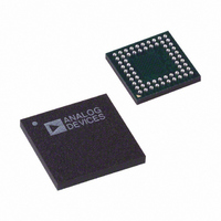
AD9929BBCZ Analog Devices Inc, AD9929BBCZ Datasheet - Page 18

AD9929BBCZ
Manufacturer Part Number
AD9929BBCZ
Description
IC CCD SIGNAL PROCESSOR 64-BGA
Manufacturer
Analog Devices Inc
Type
CCD Signal Processor, 12-Bitr
Datasheet
1.AD9929BBCZ.pdf
(64 pages)
Specifications of AD9929BBCZ
Input Type
Logic
Output Type
Logic
Interface
3-Wire Serial
Mounting Type
Surface Mount
Package / Case
64-CSPBGA
Analog Front End Type
CCD
Analog Front End Category
Video
Interface Type
Serial (3-Wire)
Input Voltage Range
0.5V
Operating Supply Voltage (min)
2.7V
Operating Supply Voltage (typ)
3V
Operating Supply Voltage (max)
3.6V
Resolution
12b
Number Of Adc's
1
Power Supply Type
Analog/Digital
Operating Temp Range
-20C to 85C
Operating Temperature Classification
Commercial
Mounting
Surface Mount
Pin Count
64
Package Type
CSPBGA
Number Of Channels
1
Lead Free Status / RoHS Status
Lead free / RoHS Compliant
Current - Supply
-
Lead Free Status / RoHS Status
Compliant, Lead free / RoHS Compliant
Available stocks
Company
Part Number
Manufacturer
Quantity
Price
Company:
Part Number:
AD9929BBCZ
Manufacturer:
ADI
Quantity:
531
AD9929
SYSTEM OVERVIEW
Figure 7 shows the typical system block diagram for the
AD9929. The CCD output is processed by the AD9929’s AFE
circuitry, which consists of a CDS, VGA, black level clamp, and
an A/D converter. The digitized pixel information is sent to the
digital image processor chip, which performs post-processing
and compression. To operate the CCD, all CCD timing para-
meters are programmed into the AD9929 from the system
microprocessor through the 3-wire serial interface. From the
system master clock, CLI, provided by the image processor or
external crystal, the AD9929 generates all of the CCDs hori-
zontal and vertical clocks and all internal AFE clocks. External
synchronization is provided by a SYNC pulse from the
CCD
CCDIN
SUBCK
VSUB
RG
V1
V2
V3
V4
H1
H2
Figure 7. Typical System Block Diagram, Master Mode
VERTICAL
DRIVER
µP
Rev. A | Page 18 of 64
AD9929
XSUBCK
XVSG1
XVSG2
XV1
XV2
XV3
XV4
microprocessor, which resets internal counters and resyn-
chronizes the VD and HD outputs.
The H-drivers for H1 to H2, and RG are included in the
AD9929, allowing these clocks to be directly connected to the
CCD. An H-drive voltage of up to 3.6 V is supported. The
AD9929 also includes the CCD vertical driver circuits for
creating the V1 to V4, and SUBCK outputs that allow direct
connection to the CCD. The AD9929 also provides program-
mable MSHUT and STROBE outputs, which may be used to
trigger mechanical shutter and strobe (flash) circuitry.
GENERATOR
TIMING
DOUT [11:0]
VGATE
DCLK1
HD, VD
FD
CLI
PROCESSING
DIGITAL
IMAGE
ASIC


