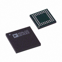
AD9929BBCZ Analog Devices Inc, AD9929BBCZ Datasheet - Page 20

AD9929BBCZ
Manufacturer Part Number
AD9929BBCZ
Description
IC CCD SIGNAL PROCESSOR 64-BGA
Manufacturer
Analog Devices Inc
Type
CCD Signal Processor, 12-Bitr
Datasheet
1.AD9929BBCZ.pdf
(64 pages)
Specifications of AD9929BBCZ
Input Type
Logic
Output Type
Logic
Interface
3-Wire Serial
Mounting Type
Surface Mount
Package / Case
64-CSPBGA
Analog Front End Type
CCD
Analog Front End Category
Video
Interface Type
Serial (3-Wire)
Input Voltage Range
0.5V
Operating Supply Voltage (min)
2.7V
Operating Supply Voltage (typ)
3V
Operating Supply Voltage (max)
3.6V
Resolution
12b
Number Of Adc's
1
Power Supply Type
Analog/Digital
Operating Temp Range
-20C to 85C
Operating Temperature Classification
Commercial
Mounting
Surface Mount
Pin Count
64
Package Type
CSPBGA
Number Of Channels
1
Lead Free Status / RoHS Status
Lead free / RoHS Compliant
Current - Supply
-
Lead Free Status / RoHS Status
Compliant, Lead free / RoHS Compliant
Available stocks
Company
Part Number
Manufacturer
Quantity
Price
Company:
Part Number:
AD9929BBCZ
Manufacturer:
ADI
Quantity:
531
AD9929
SERIAL INTERFACE TIMING
All of the internal registers of the AD9929 are accessed through
a 3-wire serial interface. The 3-wire interface consists of a clock
(SCK), serial load (SL), and serial data (SDATA).
The AD9929 has three different register types that are confi-
gured by the 3-wire serial interface. As described in Table 13,
the three register types are control registers, system registers,
and mode registers.
Table 13. Types of Serial Interface Registers
Register
Control
System
Mode_A
Mode_B
Registers
Control Register Serial Interface
The control register 3-wire interface timing requirements are
shown in Figure 10. Control data must be written into the
device one address at a time due to the noncontiguous address
spacing for the control registers. This requires writing 8 bits of
address data followed by 24 bits of configuration data between
each active low period of SL for each address. The SL signal
must be kept high for at least one full SCK cycle between
successive writes to control registers.
System Register Serial Interface
There are seventeen 32-bit system registers that are accessed
sequentially at Address 0x14, beginning with Sys_Reg [0]. When
SDATA
Address
0x00 to
0xD6
0x14
0x15
0x16
SCK
SL
NOTES
1. SDATA BITS ARE INTERNALLY LATCHED ON THE RISING EDGES OF SCK.
2. SYSTEM UPDATE OF LOADED REGISTERS OCCURS ON SL RISING EDGE.
3. THIS TIMING PATTERN MUST BE WRITTEN FOR EACH REGISTER WRITE WITH SL REMAINING HIGH FOR AT
t
DS
LEAST ONE FULL SCK PERIOD BEFORE ASSERTING SL LOW AGAIN FOR THE NEXT REGISTER WRITE.
Number of Registers
24-Bit Registers at Each Address. Not All
Addresses Are Used. See Table 8.
Seventeen 32-Bit System Registers at
Address 0x14. See Table 9.
Eight 32-bit Mode_A Registers at Address
0x15. See Table 10.
Eight 32-Bit Mode_B Registers at Address
0x16. See Table 11.
A7
1
t
LS
A6
2
t
DH
A5
3
A4
Figure 10. 3-Wire Serial Interface Timing for Control Registers
4
A3
5
A2
6
Rev. A | Page 20 of 64
A1
7
A0
8
D23
writing to the system registers, SDATA contains the 8-bit
Address 0x14, followed by Number Writes N [23:0], followed by
the Sys_Reg [31:0] data, as shown in Figure 5. The system
register map is listed in Table 9.
The value of the Number Writes N [23:0] word determines one
of two options when writing to the system registers. If Number
Writes N[23:0] = 0x000000, the device enters a mode where it
expects all 17 Sys_Reg [31:0] data-words to be clocked in before
SL is asserted high. If the Number Writes N [23:0] is decoded as
some number N other than 0x000000, then the device expects
N number of registers to be programmed, where N equals the
value of Number Writes N [23:0]. For example: if Number
Writes N[23:0] = 0x000004, the device would expect data to be
provided for Sys_Reg [3:0]. In all cases, the system registers are
written beginning with Sys_Reg [0], regardless of the value of
Number Writes N [23:0]. Note that SL can be brought high or
low during access to system registers, as shown in Figure 11.
Mode_A and Mode_B Register Serial Interface
There are eight 32-bit Mode_A and eight 32-bit Mode_B
registers that get accessed sequentially at Address 0x15 and
Address 0x16, respectively. Mode_A and Mode_B registers are
written to in exactly the same way as the system registers, as
explained previously. The mode registers are listed in Table 10
and Table 11.
To change operation between Mode_A and Mode_B, set the
1-bit mode register (Address 0x0A). The desired Mode_A
(Address 0x15) or Mode_B (Address 0x16) data must be
programmed into the Mode_A or Mode_B registers before
changing the mode bit.
9
D22
10
D21
11
....
....
D3
29
D2
30
D1
31
t
LH
D0
32


