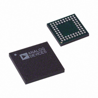
AD9929BBCZ Analog Devices Inc, AD9929BBCZ Datasheet - Page 54

AD9929BBCZ
Manufacturer Part Number
AD9929BBCZ
Description
IC CCD SIGNAL PROCESSOR 64-BGA
Manufacturer
Analog Devices Inc
Type
CCD Signal Processor, 12-Bitr
Datasheet
1.AD9929BBCZ.pdf
(64 pages)
Specifications of AD9929BBCZ
Input Type
Logic
Output Type
Logic
Interface
3-Wire Serial
Mounting Type
Surface Mount
Package / Case
64-CSPBGA
Analog Front End Type
CCD
Analog Front End Category
Video
Interface Type
Serial (3-Wire)
Input Voltage Range
0.5V
Operating Supply Voltage (min)
2.7V
Operating Supply Voltage (typ)
3V
Operating Supply Voltage (max)
3.6V
Resolution
12b
Number Of Adc's
1
Power Supply Type
Analog/Digital
Operating Temp Range
-20C to 85C
Operating Temperature Classification
Commercial
Mounting
Surface Mount
Pin Count
64
Package Type
CSPBGA
Number Of Channels
1
Lead Free Status / RoHS Status
Lead free / RoHS Compliant
Current - Supply
-
Lead Free Status / RoHS Status
Compliant, Lead free / RoHS Compliant
Available stocks
Company
Part Number
Manufacturer
Quantity
Price
Company:
Part Number:
AD9929BBCZ
Manufacturer:
ADI
Quantity:
531
AD9929
POWER SUPPLY SEQUENCING
The recommended power-up and power-down sequences are
shown in Figure 64 and Figure 65, respectively. As shown, the
VM1 and VM2 voltage level should never exceed the VH1 and
VH2 voltage level during power-up or power-down. Excessive
current results if this requirement is not met due to a PN
junction diode turning on between the VM1/2 and VH supply
pins.
Figure 63 describes the AD9929 AFETG and V-driver supplies
associated with vertical driver outputs.
GENERATOR
TIMING
Figure 63. Block Diagram of AD9929 Showing
XSUBCK
XV1
XV2
XV3
XV4
XVSG1
XVSG2
Timing Generator and Vertical Driver
0V
V-DRIVER
LOGIC
VH1 = VH2 = 15.0V
VDD = DVDD = DRVDD = HVDD = RGVDD = TCVDD = AVDD = 3V
VM1 = VM2 = –0.5V
VL = –7.5V
1
SAME TIME AS VM AND VH OR EARLIER, BUT NOT AFTER VDD.
2
V1 (VH1, VM1, VL)
V2 (VM2, VL)
V3 (VH1, VM1, VL)
V4 (VM2, VL)
SUBCK (VH2, VL)
Figure 65. Power-Down Supply Sequencing
Figure 64. Power-Up Supply Sequencing
SAME TIME AS VM AND VH OR EARLIER, BUT NOT BEFORE VDD REACHES 3V.
Rev. A | Page 54 of 64
VDD = DVDD = DRVDD = HVDD = RGVDD = TCVDD = AVDD = 3V
RECOMMENDED POWER-UP SUPPLY
SEQUENCING
When the AD9929 is powered up, the following power supply
sequence is recommended. Refer to Figure 64.
1.
2.
Caution:
There is a PN junction diode from VM1 and VM2 to VH.
Excessive current occurs if the VM1 and VM2 supply level is
greater than VH1 and VH2 supplies.
RECOMMENDED POWER-DOWN SUPPLY
SEQUENCING
When the AD9929 is powered down, the following power
supply sequence is recommended. Refer to Figure 65.
1.
2.
Turn ON: VDD, DVDD, DRVDD, HVDD, RGVDD,
TCVDD, and AVDD.
Turn ON: VH1 VH2, VM1,VM2, and VL.
Turn OFF: VH1, VH2, VM1, VM2, and VL.
Turn OFF: VDD, DVDD, DRVDD, HVDD, RGVDD,
TCVDD, and AVDD.
1
VM1 = VM2 = –0.5V
VH1 = VH2 = 15.0V
VL = –7.5V
2
0V


