AD9929BBCZ Analog Devices Inc, AD9929BBCZ Datasheet - Page 22
AD9929BBCZ
Manufacturer Part Number
AD9929BBCZ
Description
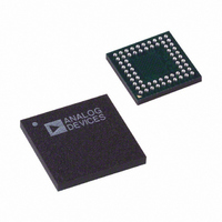
IC CCD SIGNAL PROCESSOR 64-BGA
Manufacturer
Analog Devices Inc
Type
CCD Signal Processor, 12-Bitr
Datasheet
1.AD9929BBCZ.pdf
(64 pages)
Specifications of AD9929BBCZ
Input Type
Logic
Output Type
Logic
Interface
3-Wire Serial
Mounting Type
Surface Mount
Package / Case
64-CSPBGA
Analog Front End Type
CCD
Analog Front End Category
Video
Interface Type
Serial (3-Wire)
Input Voltage Range
0.5V
Operating Supply Voltage (min)
2.7V
Operating Supply Voltage (typ)
3V
Operating Supply Voltage (max)
3.6V
Resolution
12b
Number Of Adc's
1
Power Supply Type
Analog/Digital
Operating Temp Range
-20C to 85C
Operating Temperature Classification
Commercial
Mounting
Surface Mount
Pin Count
64
Package Type
CSPBGA
Number Of Channels
1
Lead Free Status / RoHS Status
Lead free / RoHS Compliant
Current - Supply
-
Lead Free Status / RoHS Status
Compliant, Lead free / RoHS Compliant
Available stocks
Company
Part Number
Manufacturer
Quantity
Price
Company:

Part Number:
AD9929BBCZ
Manufacturer:
ADI
Quantity:
531


AD9929
ANALOG FRONT END DESCRIPTION AND
OPERATION
The AD9929 AFE signal processing chain is shown in Figure 13.
Each processing step is essential in achieving a high quality
image from the raw CCD pixel data. Registers for the AD9929
AFE section are listed in Table 14.
Table 14. AFE Registers
Register
Name
VGAGAIN
REFBLACK
AFESTBY
0.1µF
Bit
Width
10
6
1
CCDIN
Register Type
Control (Address 0x0E)
Control (Address 0x04)
Control (Address 0x05)
DC RESTORE
1.5V
SHP
CDS
SHD
Description
VGA Gain
Black Clamp
Level
AFE Standby
SHP
GENERATION
PRECISION
Figure 13. AFE Block Diagram
TIMING
SHD
6dB TO 40dB
Rev. A | Page 22 of 64
REGISTER
VGA GAIN
VGA
PHASE
DOUT
10
DC Restore
To reduce the large dc offset of the CCD output signal, a dc-
restore circuit is used with an external 0.1 µF series coupling
capacitor. This restores the dc level of the CCD signal to
approximately 1.5 V, to be compatible with the 3 V analog
supply of the AD9929.
Correlated Double Sampler
The CDS circuit samples each CCD pixel twice to extract the
video information and reject low frequency noise. The timing
shown in Figure 16 illustrates how the two internally generated
CDS clocks, SHP and SHD, are used to sample the reference and
data levels, respectively, of the CCD signal. The placement of the
SHP and SHD sampling edges is determined by the setting of
the SHPLOC (Address 0x02) and SHDLOC (Address 0x02)
registers. Placement of these two clock edges is critical in
achieving the best performance from the CCD.
8-BIT
DAC
GENERATION
CLPOB
TIMING
V-H
DIGITAL
FILTER
REFB
1.0V
OPTICAL BLACK
INTERNAL
CLAMP
ADC
1.0µF
V
2V FULL
SCALE
REF
CLAMP LEVEL
REGISTER
REFT
2.0V
1.0µF
CLPOB
8
OUTPUT
LATCH
DATA
PHASE
DOUT
12
DOUT
Related parts for AD9929BBCZ
Image
Part Number
Description
Manufacturer
Datasheet
Request
R


Part Number:
Description:
±1.7g Dual-Axis IMEMS Accelerometer Evaluation Board
Manufacturer:
Analog Devices Inc
Datasheet:

Part Number:
Description:
Inertial Sensor Evaluation System
Manufacturer:
Analog Devices Inc
Datasheet:
Part Number:
Description:
Manufacturer:
Analog Devices Inc
Datasheet:
Part Number:
Description:
Manufacturer:
Analog Devices Inc
Datasheet:
Part Number:
Description:
Manufacturer:
Analog Devices Inc
Datasheet:
Part Number:
Description:
Manufacturer:
Analog Devices Inc
Datasheet:
Part Number:
Description:
Manufacturer:
Analog Devices Inc
Datasheet:
Part Number:
Description:
Manufacturer:
Analog Devices Inc
Datasheet:
Part Number:
Description:
Manufacturer:
Analog Devices Inc
Datasheet:
Part Number:
Description:
Manufacturer:
Analog Devices Inc
Datasheet:
Part Number:
Description:
Manufacturer:
Analog Devices Inc
Datasheet:
Part Number:
Description:
Manufacturer:
Analog Devices Inc
Datasheet: