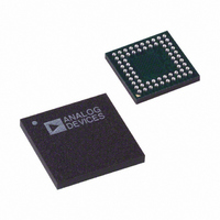
AD9929BBCZ Analog Devices Inc, AD9929BBCZ Datasheet - Page 24

AD9929BBCZ
Manufacturer Part Number
AD9929BBCZ
Description
IC CCD SIGNAL PROCESSOR 64-BGA
Manufacturer
Analog Devices Inc
Type
CCD Signal Processor, 12-Bitr
Datasheet
1.AD9929BBCZ.pdf
(64 pages)
Specifications of AD9929BBCZ
Input Type
Logic
Output Type
Logic
Interface
3-Wire Serial
Mounting Type
Surface Mount
Package / Case
64-CSPBGA
Analog Front End Type
CCD
Analog Front End Category
Video
Interface Type
Serial (3-Wire)
Input Voltage Range
0.5V
Operating Supply Voltage (min)
2.7V
Operating Supply Voltage (typ)
3V
Operating Supply Voltage (max)
3.6V
Resolution
12b
Number Of Adc's
1
Power Supply Type
Analog/Digital
Operating Temp Range
-20C to 85C
Operating Temperature Classification
Commercial
Mounting
Surface Mount
Pin Count
64
Package Type
CSPBGA
Number Of Channels
1
Lead Free Status / RoHS Status
Lead free / RoHS Compliant
Current - Supply
-
Lead Free Status / RoHS Status
Compliant, Lead free / RoHS Compliant
Available stocks
Company
Part Number
Manufacturer
Quantity
Price
Company:
Part Number:
AD9929BBCZ
Manufacturer:
ADI
Quantity:
531
AD9929
As shown in Figure 17, the H2 output is the inverse of H1. The
internal propagation delay resulting from the signal inversion is
less than 1 ns, which is significantly less than the typical rise
Table 15. RG, H1, SHP, SHD, DCLK, and DOUTPHASE Timing Parameters
Register Name
RGNEGLOC
H1POSLOC
SHPLOC
SHDLOC
DOUTPHASE
DCLKPHASE
1
The two MSB bits are used to select the quadrant
1
1
POSITION
1
1
1 PIXEL
PERIOD
1
CLI
(INTERNAL)
NOTES
1. PIXEL CLOCK PERIOD IS DIVIDED INTO 48 POSITIONS, PROVIDING FINE EDGE RESOLUTION FOR HIGH SPEED CLOCKS.
2. THERE IS A FIXED DELAY FROM THE CLI INPUT TO THE INTERNAL PIXEL PERIOD POSITIONS (
t
CLIDLY
SIGNAL
Bit Width
6b
6b
6b
6b
6b
6b
CCD
CDS
RG
H1
H2
PROGRAMMABLE CLOCK POSITIONS
1. RG RISING EDGE (FIXED EDGE AT 000000)
2. RG FALLING EDGE (RGNEGLOC (ADDRESS 0x03))
3. SHP SAMPLE LOCATION (SHPLOC (ADDRESS 0x02))
4. SHD SAMPLE LOCATION (SHDLOC (ADDRESS 0x02))
5. H1 RISING EDGE LOCATION (H1POSLOC (ADDRESS 0x03))
6. H1 NEGATIVE EDGE LOCATION (FIXED AT (H1POSLOC + 24 STEPS))
7. H2 IS ALWAYS THE INVERSE OF H1
1
5
P[0]
2
Control (Address 0x02)
Register Type
Control (Address 0x03)
Control (Address 0x03)
Control (Address 0x02)
Control (Address 0x02)
Control (Address 0x02)
Figure 15. High Speed Clock Resolution from CLI Master Clock Input
3
6
Figure 16. High Speed Clock Programmable Locations
P[12]
4
Rev. A | Page 24 of 64
Range
0 to 47 Edge Location
0 to 47 Edge Location
0 to 47 Edge Location
0 to 47 Edge Location
0 to 47 Edge Location
0 to 47 Edge Location
P[24]
time driving the CCD load. This results in a H1/H2 crossover
voltage at approximately 50% of the output swing. The
crossover voltage is not programmable.
P[36]
Description
Falling Edge Location for RG
Positive Edge Location for H1
Sample Location for SHP
Sample Location for SHD
Phase Location of Data Output [9:0]
Positive Edge of DCLK 1
t
CLIDLY
= 6ns TYP).
P[48] = P[0]


