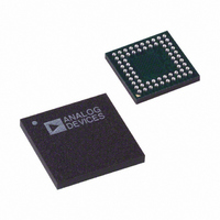
AD9929BBCZ Analog Devices Inc, AD9929BBCZ Datasheet - Page 55

AD9929BBCZ
Manufacturer Part Number
AD9929BBCZ
Description
IC CCD SIGNAL PROCESSOR 64-BGA
Manufacturer
Analog Devices Inc
Type
CCD Signal Processor, 12-Bitr
Datasheet
1.AD9929BBCZ.pdf
(64 pages)
Specifications of AD9929BBCZ
Input Type
Logic
Output Type
Logic
Interface
3-Wire Serial
Mounting Type
Surface Mount
Package / Case
64-CSPBGA
Analog Front End Type
CCD
Analog Front End Category
Video
Interface Type
Serial (3-Wire)
Input Voltage Range
0.5V
Operating Supply Voltage (min)
2.7V
Operating Supply Voltage (typ)
3V
Operating Supply Voltage (max)
3.6V
Resolution
12b
Number Of Adc's
1
Power Supply Type
Analog/Digital
Operating Temp Range
-20C to 85C
Operating Temperature Classification
Commercial
Mounting
Surface Mount
Pin Count
64
Package Type
CSPBGA
Number Of Channels
1
Lead Free Status / RoHS Status
Lead free / RoHS Compliant
Current - Supply
-
Lead Free Status / RoHS Status
Compliant, Lead free / RoHS Compliant
Available stocks
Company
Part Number
Manufacturer
Quantity
Price
Company:
Part Number:
AD9929BBCZ
Manufacturer:
ADI
Quantity:
531
INITIAL START-UP SEQUENCE
Recommended Start-Up Sequence for Master Mode
When the AD9929 is powered up, the following sequence is
recommended (refer to Figure 66 for each step).
1.
2.
3.
4.
(INTERNAL SIGNAL)
Turn on power supplies as described in the Power Supply
Sequencing section.
Apply the CLI master clock input.
CLI is output on DCLK2 Pin 16 at this time.
Reset the internal AD9929 registers. Write a 0x000000 to
the SW_RESET register (Address 0x00). This sets all
internal register values to their default values. (This step is
optional because there is an internal power-on reset circuit
that is applied at power-up.)
Program DIGSTBY and AFESTBY registers (Address 0x05)
= 1 and all other necessary control registers.
SEQUENCE
POWER-UP
OUTCONT
(OUTPUTS)
(OUTPUT)
(OUTPUT)
(OUTPUT)
(OUTPUT)
DIGITAL
WRITES
DCLK2
AD9929
(INPUT)
SERIAL
DCLK1
CLI
VD
HD
1
2
NOTES
1
2
3
4
OUTCONT IS AN INTERNAL SIGNAL THAT IS CONTROLLED USING REGISTER OUTCONT_REG (ADDRESS 0x05).
DCLK2 WILL BE OUTPUT ON THE FD/DCLK2 PIN 16 PROVIDING REGISTER DCLK2SEL (ADDRESS 0xD5) = 1.
IT TAKES 11 CLI CLOCKS FROM WHEN OCONT GOES HIGH UNTIL VD, HD, AND DIGITAL OUTPUT DATA IS VALID.
THERE IS A 500µS SETTLING TIME FROM WHEN THE DIGSTBY REGISTER IS SET TO WHEN THE DCLK1 IS STABLE.
THE DCLK2SEL REGISTER DEFAULTS TO 1 AT POWER-UP.
t
PWR
H1, VSUB, FD
H2, RG, MSHUT, STROBE
3
Figure 66. Recommended Start-Up Sequence and Synchronization, Master Mode
t
SETTLING
5
4
7
Rev. A | Page 55 of 64
t
DELAY
3
1 H
ODD FIELD
5.
6.
7.
8.
9.
10. Program control register MODE (Address 0x0A) = 1. This
Program system registers (Address 0x20).
Program Mode_A registers (Address 0x21).
Program Mode_B registers (Address 0x22).
Program OUTCONT_REG register (Address 0x05) = 1.
(The internal OUTCONT signal is asserted high at this
time. This enables the digital outputs.)
Program control register MODE (Address 0x0A) = 0. This
selects Mode_A operation. (This step is optional because
the AD9929 defaults to Mode_A at power-up.)
selects Mode_B operation. Note: Complete this write at
least 4 CLI cycles before the start of the next field.
1 V
EVEN FIELD
ODD FIELD
AD9929


