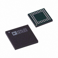
AD9929BBCZ Analog Devices Inc, AD9929BBCZ Datasheet - Page 21

AD9929BBCZ
Manufacturer Part Number
AD9929BBCZ
Description
IC CCD SIGNAL PROCESSOR 64-BGA
Manufacturer
Analog Devices Inc
Type
CCD Signal Processor, 12-Bitr
Datasheet
1.AD9929BBCZ.pdf
(64 pages)
Specifications of AD9929BBCZ
Input Type
Logic
Output Type
Logic
Interface
3-Wire Serial
Mounting Type
Surface Mount
Package / Case
64-CSPBGA
Analog Front End Type
CCD
Analog Front End Category
Video
Interface Type
Serial (3-Wire)
Input Voltage Range
0.5V
Operating Supply Voltage (min)
2.7V
Operating Supply Voltage (typ)
3V
Operating Supply Voltage (max)
3.6V
Resolution
12b
Number Of Adc's
1
Power Supply Type
Analog/Digital
Operating Temp Range
-20C to 85C
Operating Temperature Classification
Commercial
Mounting
Surface Mount
Pin Count
64
Package Type
CSPBGA
Number Of Channels
1
Lead Free Status / RoHS Status
Lead free / RoHS Compliant
Current - Supply
-
Lead Free Status / RoHS Status
Compliant, Lead free / RoHS Compliant
Available stocks
Company
Part Number
Manufacturer
Quantity
Price
Company:
Part Number:
AD9929BBCZ
Manufacturer:
ADI
Quantity:
531
VD Synchronous and Asynchronous Register Operation
There are two types of control registers, VD synchronous and
VD asynchronous, as indicated in the address column of
Table 8. Register writes to synchronous and asynchronous
registers operate differently, as described in the following
sections. All writes to system Mode_A and Mode_B registers
occur asynchronously.
Asynchronous Register Operation
For VD asynchronous register writes, SDATA data is stored
directly into the serial register at the rising edge of SL. As a
result, register operation begins immediately after the rising
edge of SL.
CLI
SDATA
HD
VD
SCK
SL
NOTES
1. SL PULSES ARE IGNORED UNTIL THE LSB BIT OF THE LAST DATA N WORD IS CLOCKED IN.
2. VALID SL PULSE. SL MUST BE ASSERTED HIGH WHEN ALL SDI DATA TRANSMISSIONS HAVE BEEN FINISHED.
8 BIT ADDRESS
ADDRESS [7:0]
PROGRAMMING VD SYNCHRONOUS
TYPE REGISTERS MUST BE
COMPLETED AT LEAST 4 CLI
CYCLES BEFORE THE FALLING
EDGE OF VD
NUMBER WRITES N [23:0]
NUMBER OF 32 BIT
DATA WRITES (N)
Figure 12. VD Synchronous Type Register Writes
Figure 11. System and Mode Register Writes
Rev. A | Page 21 of 64
DATA 1 [31:0]
1
DATA 1 [31:0]
OPERATION OF VD SYNCHRONOUS
TYPE REGISTER WRITES BEGIN AT
THE NEXT VD FALLING EDGE.
VD Synchronous Register Operation
For VD synchronous registers, SDATA data is temporarily
stored in a buffer register at the rising edge of SL. This data is
held in the buffer register until the next falling edge of VD is
applied. Once the next falling edge of VD occurs, the buffered
SDATA data is loaded into the serial register, at which time the
register operation begins. See Figure 12.
All control registers at the following addresses are VD synchro-
nous type registers: Addresses 0x0A, 0x0B, 0x0C, 0x0D, and
0x0E. Also see Table 8, the Control Register Address Map.
1
DATA 2 [31:0]
DATA 2 [31:0]
12
DATA N [31:0]
DATA N [31:0]
AD9929


