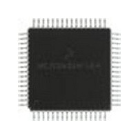
MC68HC908LD60IFU Freescale Semiconductor, MC68HC908LD60IFU Datasheet - Page 161

MC68HC908LD60IFU
Manufacturer Part Number
MC68HC908LD60IFU
Description
Manufacturer
Freescale Semiconductor
Datasheet
1.MC68HC908LD60IFU.pdf
(292 pages)
Specifications of MC68HC908LD60IFU
Cpu Family
HC08
Device Core Size
8b
Frequency (max)
6MHz
Program Memory Type
Flash
Program Memory Size
60KB
Total Internal Ram Size
1KB
# I/os (max)
39
Number Of Timers - General Purpose
2
Operating Supply Voltage (typ)
3.3V
Operating Supply Voltage (max)
3.6V
Operating Supply Voltage (min)
3V
On-chip Adc
6-chx8-bit
Instruction Set Architecture
CISC
Operating Temp Range
0C to 85C
Operating Temperature Classification
Commercial
Mounting
Surface Mount
Pin Count
64
Package Type
PQFP
Lead Free Status / Rohs Status
Compliant
Available stocks
Company
Part Number
Manufacturer
Quantity
Price
- Current page: 161 of 292
- Download datasheet (4Mb)
MC68HC908LD60
Freescale Semiconductor
NOTE:
NOTE:
—
Rev. 1.1
Before changing a channel function by writing to the MSxB or MSxA bit,
set the TSTOP and TRST bits in the TIM status and control register
(TSC).
ELSxB and ELSxA — Edge/Level Select Bits
Before enabling a TIM channel register for input capture operation, make
sure that the TCHx pin is stable for at least two bus clocks.
Notes:
MSxB
1. For CLAMP/TCH0 pin only.
When channel x is an input capture channel, these read/write bits
control the active edge-sensing logic on channel x.
When channel x is an output compare channel, ELSxB and ELSxA
control the channel x output behavior when an output compare
occurs.
When ELS0B and ELS0A are both clear, channel 0 is not connected
to the CLAMP/TCH0 pin. The pin is available as the CLAMP output of
the sync processor.
Table 11-3
ELSxB and ELSxA bits.
X
X
0
0
0
0
0
0
1
1
1
MSxA
0
1
0
0
0
1
1
1
X
X
X
Timer Interface Module (TIM)
Table 11-3. Mode, Edge, and Level Selection
shows how ELSxB and ELSxA work. Reset clears the
ELSxB
0
0
0
1
1
0
1
1
0
1
1
ELSxA
0
0
1
0
1
1
0
1
1
0
1
Compare or
Compare
Capture
or PWM
Buffered
Buffered
Output
Output
Mode
Preset
Output
Input
PWM
Pin is CLAMP of sync processor
Initial Output Level High
Pin is CLAMP of sync processor
Initial Output Level Low
Capture on Rising Edge Only
Capture on Falling Edge Only
Capture on Rising or Falling Edge
Toggle Output on Compare
Clear Output on Compare
Set Output on Compare
Toggle Output on Compare
Clear Output on Compare
Set Output on Compare
Timer Interface Module (TIM)
Configuration
Technical Data
I/O Registers
(1)
(1)
161
;
;
Related parts for MC68HC908LD60IFU
Image
Part Number
Description
Manufacturer
Datasheet
Request
R
Part Number:
Description:
Manufacturer:
Freescale Semiconductor, Inc
Datasheet:
Part Number:
Description:
Manufacturer:
Freescale Semiconductor, Inc
Datasheet:
Part Number:
Description:
Manufacturer:
Freescale Semiconductor, Inc
Datasheet:
Part Number:
Description:
Manufacturer:
Freescale Semiconductor, Inc
Datasheet:
Part Number:
Description:
Manufacturer:
Freescale Semiconductor, Inc
Datasheet:
Part Number:
Description:
Manufacturer:
Freescale Semiconductor, Inc
Datasheet:
Part Number:
Description:
Manufacturer:
Freescale Semiconductor, Inc
Datasheet:
Part Number:
Description:
Manufacturer:
Freescale Semiconductor, Inc
Datasheet:
Part Number:
Description:
Manufacturer:
Freescale Semiconductor, Inc
Datasheet:
Part Number:
Description:
Manufacturer:
Freescale Semiconductor, Inc
Datasheet:
Part Number:
Description:
Manufacturer:
Freescale Semiconductor, Inc
Datasheet:
Part Number:
Description:
Manufacturer:
Freescale Semiconductor, Inc
Datasheet:
Part Number:
Description:
Manufacturer:
Freescale Semiconductor, Inc
Datasheet:
Part Number:
Description:
Manufacturer:
Freescale Semiconductor, Inc
Datasheet:
Part Number:
Description:
Manufacturer:
Freescale Semiconductor, Inc
Datasheet:


