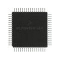
MC68HC908LD60IFU Freescale Semiconductor, MC68HC908LD60IFU Datasheet - Page 59

MC68HC908LD60IFU
Manufacturer Part Number
MC68HC908LD60IFU
Description
Manufacturer
Freescale Semiconductor
Datasheet
1.MC68HC908LD60IFU.pdf
(292 pages)
Specifications of MC68HC908LD60IFU
Cpu Family
HC08
Device Core Size
8b
Frequency (max)
6MHz
Program Memory Type
Flash
Program Memory Size
60KB
Total Internal Ram Size
1KB
# I/os (max)
39
Number Of Timers - General Purpose
2
Operating Supply Voltage (typ)
3.3V
Operating Supply Voltage (max)
3.6V
Operating Supply Voltage (min)
3V
On-chip Adc
6-chx8-bit
Instruction Set Architecture
CISC
Operating Temp Range
0C to 85C
Operating Temperature Classification
Commercial
Mounting
Surface Mount
Pin Count
64
Package Type
PQFP
Lead Free Status / Rohs Status
Compliant
Available stocks
Company
Part Number
Manufacturer
Quantity
Price
- Current page: 59 of 292
- Download datasheet (4Mb)
4.4.1 13k-Byte FLASH Even Byte Write Buffer (13KEBUF)
4.5 FLASH Block Erase Operation
MC68HC908LD60
Freescale Semiconductor
NOTE:
—
Rev. 1.1
Address:
Bit[7:0] — 13k-Byte FLASH Even Write Byte Buffer
The minimum erase size for the FLASH memory is one block, and is
carried out by the block erase operation. For memory $0C00–$0FFF, a
block consists of 128 consecutive bytes starting from addresses $xx00
or $xx80. For memory $1000–$3FFF and $4000–$F9FF, a block
consists of 512 consecutive bytes starting from addresses $x000,
$x200, $x400, $x600, $x800, $xA00, $xC00, or $xE00.
The 32-byte user vectors, $FFE0–$FFFF, cannot be erased by the block
erase operation because of security reasons. Mass erase is required to
erase this block.
Use the following procedure to erase a block of FLASH memory:
Figure 4-4. 13k-Byte FLASH Even Byte Write Buffer (13KEBUF)
Reset:
Read:
Write:
1. Set the ERASE bit, and clear the MASS bit in the FLASH control
2. Write any data to any FLASH address within the block address
3. Wait for a time, t
Data is written to this buffer to be programmed to an even location of
the 13k-byte array. The byte gets programmed to the FLASH memory
when the odd location is programmed. Even locations are $0C00,
$0CDE, $1000, etc; the corresponding odd locations are $0C01,
$0CDF, $1001, etc. The 13k-byte array are locations from $0C00 to
$3FFF. Reset has no effect on these bits.
register.
range desired.
$0066
Bit 7
Bit7
Bit6
FLASH Memory
6
nvs
Bit5
(min. 5µs)
5
Unaffected by reset
Bit4
4
Bit3
3
FLASH Block Erase Operation
Bit2
2
Bit1
FLASH Memory
1
Technical Data
Bit0
0
59
Related parts for MC68HC908LD60IFU
Image
Part Number
Description
Manufacturer
Datasheet
Request
R
Part Number:
Description:
Manufacturer:
Freescale Semiconductor, Inc
Datasheet:
Part Number:
Description:
Manufacturer:
Freescale Semiconductor, Inc
Datasheet:
Part Number:
Description:
Manufacturer:
Freescale Semiconductor, Inc
Datasheet:
Part Number:
Description:
Manufacturer:
Freescale Semiconductor, Inc
Datasheet:
Part Number:
Description:
Manufacturer:
Freescale Semiconductor, Inc
Datasheet:
Part Number:
Description:
Manufacturer:
Freescale Semiconductor, Inc
Datasheet:
Part Number:
Description:
Manufacturer:
Freescale Semiconductor, Inc
Datasheet:
Part Number:
Description:
Manufacturer:
Freescale Semiconductor, Inc
Datasheet:
Part Number:
Description:
Manufacturer:
Freescale Semiconductor, Inc
Datasheet:
Part Number:
Description:
Manufacturer:
Freescale Semiconductor, Inc
Datasheet:
Part Number:
Description:
Manufacturer:
Freescale Semiconductor, Inc
Datasheet:
Part Number:
Description:
Manufacturer:
Freescale Semiconductor, Inc
Datasheet:
Part Number:
Description:
Manufacturer:
Freescale Semiconductor, Inc
Datasheet:
Part Number:
Description:
Manufacturer:
Freescale Semiconductor, Inc
Datasheet:
Part Number:
Description:
Manufacturer:
Freescale Semiconductor, Inc
Datasheet:


