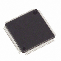
DS2156L+ Maxim Integrated Products, DS2156L+ Datasheet - Page 187

DS2156L+
Manufacturer Part Number
DS2156L+
Description
IC TXRX T1/E1/J1 1-CHIP 100-LQFP
Manufacturer
Maxim Integrated Products
Datasheet
1.DS2156L.pdf
(265 pages)
Specifications of DS2156L+
Function
Single-Chip Transceiver
Interface
E1, J1, T1, TDM, UTOPIA II
Number Of Circuits
1
Voltage - Supply
3.14 V ~ 3.47 V
Current - Supply
75mA
Operating Temperature
0°C ~ 70°C
Mounting Type
Surface Mount
Package / Case
100-LQFP
Includes
BERT Generator and Detector, CMI Coder and Decoder, HDLC Controller
Lead Free Status / RoHS Status
Lead free / RoHS Compliant
Power (watts)
-
- Current page: 187 of 265
- Download datasheet (2Mb)
Register Name:
Register Description:
Register Address:
Bit #
Name
Default
Bits 0 to 7/Receive LCD Integration Period (RLIP0 to RLIP7)
This 8-bit register holds the LCD integration period value for which the out-of-cell delineation condition must
persist for declaring loss-of-cell delineation (LCD). For deasserting LCD, cell delineation should persist in the
SYNC state for the same amount of time programmed in this register. LCD state change condition can be
programmed to generate an external interrupt through U_RCR2.4. A value of 0 programmed into this register
declares LCD for every OCD condition at the resolution of the internal system clock period. The internal system
clock is 8x the line clock [16.383MHz (E1 mode) and 12.352MHz (T1 mode)].
For example, in E1 mode a register value of 64h (100) generates a 100ms integration time. In T1 mode, a register
value of 4Bh (75) generates a 100ms integration time.
Register Name:
Register Description:
Register Address:
Bit #
Name
Default
Bits 0 to 7/The host should always write 0x00 to this register when latching the receive PMON counter.
This register is provided for latching all receive PMON-counter values, namely the 16-bit receive assigned cell-
count value, 12-bit receive uncorrectable HEC-count value, and 8-bit receive correctable HEC-count value of a port
into the common receive assigned cell-counter latch register, receive uncorrectable HEC-counter latch register, and
receive correctable HEC-count latch register, respectively. A write into this register clears the receive PMON
counters for that port.
IT = Integration Time in ms
For E1 mode, register value = IT / 1ms
For T1 mode, register value = IT / 1.326ms
RLIP7
—
7
7
0
0
RLIP6
—
U_RLCDIP
UTOPIA Receive LCD Integration Period Register
61h
U_RPCE
UTOPIA Receive PMON-Counter Enable Register
62h
6
1
6
0
RLIP5
—
5
1
5
0
RLIP4
—
4
0
4
0
187 of 265
RLIP3
—
3
0
3
0
RLIP2
—
2
1
2
0
RLIP1
—
1
1
1
0
RLIP0
—
0
0
0
0
Related parts for DS2156L+
Image
Part Number
Description
Manufacturer
Datasheet
Request
R

Part Number:
Description:
Ds2156, Ds2156l, Ds2156ln T1/e1/j1 Single-chip Transceiver Tdm/utopia Ii Interface
Manufacturer:
Maxim Integrated Products, Inc.
Datasheet:

Part Number:
Description:
MAX7528KCWPMaxim Integrated Products [CMOS Dual 8-Bit Buffered Multiplying DACs]
Manufacturer:
Maxim Integrated Products
Datasheet:

Part Number:
Description:
Single +5V, fully integrated, 1.25Gbps laser diode driver.
Manufacturer:
Maxim Integrated Products
Datasheet:

Part Number:
Description:
Single +5V, fully integrated, 155Mbps laser diode driver.
Manufacturer:
Maxim Integrated Products
Datasheet:

Part Number:
Description:
VRD11/VRD10, K8 Rev F 2/3/4-Phase PWM Controllers with Integrated Dual MOSFET Drivers
Manufacturer:
Maxim Integrated Products
Datasheet:

Part Number:
Description:
Highly Integrated Level 2 SMBus Battery Chargers
Manufacturer:
Maxim Integrated Products
Datasheet:

Part Number:
Description:
Current Monitor and Accumulator with Integrated Sense Resistor; ; Temperature Range: -40°C to +85°C
Manufacturer:
Maxim Integrated Products

Part Number:
Description:
TSSOP 14/A�/RS-485 Transceivers with Integrated 100O/120O Termination Resis
Manufacturer:
Maxim Integrated Products

Part Number:
Description:
TSSOP 14/A�/RS-485 Transceivers with Integrated 100O/120O Termination Resis
Manufacturer:
Maxim Integrated Products

Part Number:
Description:
QFN 16/A�/AC-DC and DC-DC Peak-Current-Mode Converters with Integrated Step
Manufacturer:
Maxim Integrated Products

Part Number:
Description:
TDFN/A/65V, 1A, 600KHZ, SYNCHRONOUS STEP-DOWN REGULATOR WITH INTEGRATED SWI
Manufacturer:
Maxim Integrated Products

Part Number:
Description:
Integrated Temperature Controller f
Manufacturer:
Maxim Integrated Products

Part Number:
Description:
SOT23-6/I�/45MHz to 650MHz, Integrated IF VCOs with Differential Output
Manufacturer:
Maxim Integrated Products

Part Number:
Description:
SOT23-6/I�/45MHz to 650MHz, Integrated IF VCOs with Differential Output
Manufacturer:
Maxim Integrated Products

Part Number:
Description:
EVALUATION KIT/2.4GHZ TO 2.5GHZ 802.11G/B RF TRANSCEIVER WITH INTEGRATED PA
Manufacturer:
Maxim Integrated Products


