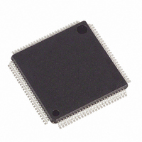
DS2156L+ Maxim Integrated Products, DS2156L+ Datasheet - Page 225

DS2156L+
Manufacturer Part Number
DS2156L+
Description
IC TXRX T1/E1/J1 1-CHIP 100-LQFP
Manufacturer
Maxim Integrated Products
Datasheet
1.DS2156L.pdf
(265 pages)
Specifications of DS2156L+
Function
Single-Chip Transceiver
Interface
E1, J1, T1, TDM, UTOPIA II
Number Of Circuits
1
Voltage - Supply
3.14 V ~ 3.47 V
Current - Supply
75mA
Operating Temperature
0°C ~ 70°C
Mounting Type
Surface Mount
Package / Case
100-LQFP
Includes
BERT Generator and Detector, CMI Coder and Decoder, HDLC Controller
Lead Free Status / RoHS Status
Lead free / RoHS Compliant
Power (watts)
-
- Current page: 225 of 265
- Download datasheet (2Mb)
33.
33.1 Description
The DS2156 IEEE 1149.1 design supports the standard instruction codes SAMPLE/PRELOAD,
BYPASS, and EXTEST. Optional public instructions included are HIGH-Z, CLAMP, and IDCODE
(Figure 33-1.). The DS2156 contains the following features as required by IEEE 1149.1 standard test
access port (TAP) and boundary scan architecture.
The DS2156 is pin-compatible with the DS2152, DS21x52 (T1) and DS2154, DS21x54 (E1) SCT
families. The JTAG feature uses pins that had no function in the DS2152 and DS2154. Details about
boundary scan architecture and the TAP are in IEEE 1149.1-1990, IEEE 1149.1a-1993, and IEEE
1149.1b-1994.
The TAP contains the necessary interface pins JTRST, JTCLK, JTMS, JTDI, and JTDO. See the pin
descriptions in Section 3 for details.
Figure 33-1. JTAG Functional Block Diagram
Test Access Port
TAP Controller
Instruction Register
Bypass Register
Boundary Scan Register
Device Identification Register
JTAG BOUNDARY SCAN ARCHITECTURE AND TEST ACCESS PORT
10kΩ
+V
JTDI
10kΩ
+V
JTMS
TEST ACCESS PORT
BOUNDARY SCAN
IDENTIFICATION
CONTROLLER
INSTRUCTION
REGISTER
REGISTER
REGISTER
REGISTER
BYPASS
JTCLK
225 of 265
10kΩ
+V
JTRST
SELECT
OUTPUT ENABLE
MUX
JTDO
Related parts for DS2156L+
Image
Part Number
Description
Manufacturer
Datasheet
Request
R

Part Number:
Description:
Ds2156, Ds2156l, Ds2156ln T1/e1/j1 Single-chip Transceiver Tdm/utopia Ii Interface
Manufacturer:
Maxim Integrated Products, Inc.
Datasheet:

Part Number:
Description:
MAX7528KCWPMaxim Integrated Products [CMOS Dual 8-Bit Buffered Multiplying DACs]
Manufacturer:
Maxim Integrated Products
Datasheet:

Part Number:
Description:
Single +5V, fully integrated, 1.25Gbps laser diode driver.
Manufacturer:
Maxim Integrated Products
Datasheet:

Part Number:
Description:
Single +5V, fully integrated, 155Mbps laser diode driver.
Manufacturer:
Maxim Integrated Products
Datasheet:

Part Number:
Description:
VRD11/VRD10, K8 Rev F 2/3/4-Phase PWM Controllers with Integrated Dual MOSFET Drivers
Manufacturer:
Maxim Integrated Products
Datasheet:

Part Number:
Description:
Highly Integrated Level 2 SMBus Battery Chargers
Manufacturer:
Maxim Integrated Products
Datasheet:

Part Number:
Description:
Current Monitor and Accumulator with Integrated Sense Resistor; ; Temperature Range: -40°C to +85°C
Manufacturer:
Maxim Integrated Products

Part Number:
Description:
TSSOP 14/A�/RS-485 Transceivers with Integrated 100O/120O Termination Resis
Manufacturer:
Maxim Integrated Products

Part Number:
Description:
TSSOP 14/A�/RS-485 Transceivers with Integrated 100O/120O Termination Resis
Manufacturer:
Maxim Integrated Products

Part Number:
Description:
QFN 16/A�/AC-DC and DC-DC Peak-Current-Mode Converters with Integrated Step
Manufacturer:
Maxim Integrated Products

Part Number:
Description:
TDFN/A/65V, 1A, 600KHZ, SYNCHRONOUS STEP-DOWN REGULATOR WITH INTEGRATED SWI
Manufacturer:
Maxim Integrated Products

Part Number:
Description:
Integrated Temperature Controller f
Manufacturer:
Maxim Integrated Products

Part Number:
Description:
SOT23-6/I�/45MHz to 650MHz, Integrated IF VCOs with Differential Output
Manufacturer:
Maxim Integrated Products

Part Number:
Description:
SOT23-6/I�/45MHz to 650MHz, Integrated IF VCOs with Differential Output
Manufacturer:
Maxim Integrated Products

Part Number:
Description:
EVALUATION KIT/2.4GHZ TO 2.5GHZ 802.11G/B RF TRANSCEIVER WITH INTEGRATED PA
Manufacturer:
Maxim Integrated Products


