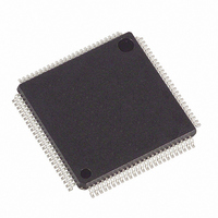
DS2156L+ Maxim Integrated Products, DS2156L+ Datasheet - Page 62

DS2156L+
Manufacturer Part Number
DS2156L+
Description
IC TXRX T1/E1/J1 1-CHIP 100-LQFP
Manufacturer
Maxim Integrated Products
Datasheet
1.DS2156L.pdf
(265 pages)
Specifications of DS2156L+
Function
Single-Chip Transceiver
Interface
E1, J1, T1, TDM, UTOPIA II
Number Of Circuits
1
Voltage - Supply
3.14 V ~ 3.47 V
Current - Supply
75mA
Operating Temperature
0°C ~ 70°C
Mounting Type
Surface Mount
Package / Case
100-LQFP
Includes
BERT Generator and Detector, CMI Coder and Decoder, HDLC Controller
Lead Free Status / RoHS Status
Lead free / RoHS Compliant
Power (watts)
-
- Current page: 62 of 265
- Download datasheet (2Mb)
9. E1 FRAMER/FORMATTER CONTROL AND STATUS REGISTERS
The E1 framer portion of the DS2156 is configured by a set of four control registers. Typically, the
control registers are only accessed when the system is first powered up. Once the DS2156 has been
initialized, the control registers need only to be accessed when there is a change in the system
configuration. There are two receive control registers (E1RCR1 and E1RCR2) and two transmit control
registers (E1TCR1 and E1TCR2). There are also four status and information registers. Each of these eight
registers is described in this section.
9.1
Register Name:
Register Description:
Register Address:
Bit #
Name
Default
Bit 0/Resync (RESYNC). When toggled from low to high, a resync is initiated. Must be cleared and set again for a
subsequent resync.
Bit 1/Sync Enable (SYNCE)
Bit 2/Frame Resync Criteria (FRC)
Bit 3/Receive CRC4 Enable (RCRC4)
Bit 4/Receive G.802 Enable (RG802). See Section 16 for details.
Bit 5/Receive HDB3 Enable (RHDB3)
Bit 6/Receive Signaling Mode Select (RSIGM)
Bit 7/RSER Control (RSERC)
E1 Control Registers
0 = auto resync enabled
1 = auto resync disabled
0 = resync if FAS received in error three consecutive times
1 = resync if FAS or bit 2 of non-FAS is received in error three consecutive times
0 = CRC4 disabled
1 = CRC4 enabled
0 = do not force RCHBLK high during bit 1 of time slot 26
1 = force RCHBLK high during bit 1 of time slot 26
0 = HDB3 disabled
1 = HDB3 enabled
0 = CAS signaling mode
1 = CCS signaling mode
0 = allow RSER to output data as received under all conditions
1 = force RSER to 1 under loss-of-frame alignment conditions
RSERC
7
0
RSIGM
E1RCR1
E1 Receive Control Register 1
33h
6
0
RHDB3
5
0
RG802
4
0
62 of 265
RCRC4
3
0
FRC
2
0
SYNCE
1
0
RESYNC
0
0
Related parts for DS2156L+
Image
Part Number
Description
Manufacturer
Datasheet
Request
R

Part Number:
Description:
Ds2156, Ds2156l, Ds2156ln T1/e1/j1 Single-chip Transceiver Tdm/utopia Ii Interface
Manufacturer:
Maxim Integrated Products, Inc.
Datasheet:

Part Number:
Description:
MAX7528KCWPMaxim Integrated Products [CMOS Dual 8-Bit Buffered Multiplying DACs]
Manufacturer:
Maxim Integrated Products
Datasheet:

Part Number:
Description:
Single +5V, fully integrated, 1.25Gbps laser diode driver.
Manufacturer:
Maxim Integrated Products
Datasheet:

Part Number:
Description:
Single +5V, fully integrated, 155Mbps laser diode driver.
Manufacturer:
Maxim Integrated Products
Datasheet:

Part Number:
Description:
VRD11/VRD10, K8 Rev F 2/3/4-Phase PWM Controllers with Integrated Dual MOSFET Drivers
Manufacturer:
Maxim Integrated Products
Datasheet:

Part Number:
Description:
Highly Integrated Level 2 SMBus Battery Chargers
Manufacturer:
Maxim Integrated Products
Datasheet:

Part Number:
Description:
Current Monitor and Accumulator with Integrated Sense Resistor; ; Temperature Range: -40°C to +85°C
Manufacturer:
Maxim Integrated Products

Part Number:
Description:
TSSOP 14/A�/RS-485 Transceivers with Integrated 100O/120O Termination Resis
Manufacturer:
Maxim Integrated Products

Part Number:
Description:
TSSOP 14/A�/RS-485 Transceivers with Integrated 100O/120O Termination Resis
Manufacturer:
Maxim Integrated Products

Part Number:
Description:
QFN 16/A�/AC-DC and DC-DC Peak-Current-Mode Converters with Integrated Step
Manufacturer:
Maxim Integrated Products

Part Number:
Description:
TDFN/A/65V, 1A, 600KHZ, SYNCHRONOUS STEP-DOWN REGULATOR WITH INTEGRATED SWI
Manufacturer:
Maxim Integrated Products

Part Number:
Description:
Integrated Temperature Controller f
Manufacturer:
Maxim Integrated Products

Part Number:
Description:
SOT23-6/I�/45MHz to 650MHz, Integrated IF VCOs with Differential Output
Manufacturer:
Maxim Integrated Products

Part Number:
Description:
SOT23-6/I�/45MHz to 650MHz, Integrated IF VCOs with Differential Output
Manufacturer:
Maxim Integrated Products

Part Number:
Description:
EVALUATION KIT/2.4GHZ TO 2.5GHZ 802.11G/B RF TRANSCEIVER WITH INTEGRATED PA
Manufacturer:
Maxim Integrated Products


