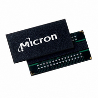
MT46H8M16LFCF-10 IT Micron Technology Inc, MT46H8M16LFCF-10 IT Datasheet - Page 10

MT46H8M16LFCF-10 IT
Manufacturer Part Number
MT46H8M16LFCF-10 IT
Description
IC DDR SDRAM 128MBIT 60VFBGA
Manufacturer
Micron Technology Inc
Type
DDR SDRAMr
Specifications of MT46H8M16LFCF-10 IT
Format - Memory
RAM
Memory Type
Mobile DDR SDRAM
Memory Size
128M (8Mx16)
Speed
100MHz
Interface
Parallel
Voltage - Supply
1.7 V ~ 1.9 V
Operating Temperature
-40°C ~ 85°C
Package / Case
60-VFBGA
Organization
8Mx16
Density
128Mb
Address Bus
15b
Access Time (max)
7ns
Maximum Clock Rate
104MHz
Operating Supply Voltage (typ)
1.8V
Package Type
VFBGA
Operating Temp Range
-40C to 85C
Operating Supply Voltage (max)
1.9V
Operating Supply Voltage (min)
1.7V
Supply Current
90mA
Pin Count
60
Mounting
Surface Mount
Operating Temperature Classification
Industrial
Lead Free Status / RoHS Status
Lead free / RoHS Compliant
Burst Type
READ Latency
Figure 3:
PDF: 09005aef822b7e27/Source: 09005aef822b7dd6
MT46H8M16LFB_2.fm - Rev. A 5/06 EN
Standard Mode Register Definition
Accesses within a given burst may be programmed to be either sequential or interleaved;
this is referred to as the burst type and is selected via bit M3.
The ordering of accesses within a burst is determined by the burst length, the burst type
and the starting column address. See Table 5 on page 11 for more information.
The READ latency is the delay, in clock cycles, between the registration of a READ
command and the availability of the first bit of output data. The latency can be set to 2 or
3 clocks, as shown in Figure 3 on page 10.
For CL = 3, if the READ command is registered at clock edge n, then the data will nomi-
nally be available at (n + 2 clocks +
clock edge n, then the data will be nominally be available at (n + 1 clock +
Reserved states should not be used as unknown operation or incompatibility with future
versions may result.
M11
0
–
Should be
programmed
to “0” to ensure
compatibility with
future devices.
M13 M12
0
0
1
1
M10
0
–
0
1
0
1
M9
0
–
Mode Register Definintion
Base Mode Register
Reserved
Extended Mode Register
Reserved
M8
0
–
M13
BA1
13
0
M7
0
–
0
12
M12
BA0
Valid
11
–
A11
M11
M6
Operating Mode
0
0
0
0
1
1
1
1
10
A10
M10
M5
Normal Operation
All other states reserved
0
0
1
1
0
0
1
1
Operating Mode
10
M4
A9
M9
9
0
1
0
1
0
1
0
1
t
M8
A8
8
AC). For CL = 2, if the READ command is registered at
128Mb: 8 Meg x 16 Mobile DDR SDRAM
CAS Latency
M7
A7
7
Reserved
Reserved
Reserved
Reserved
Reserved
Reserved
Micron Technology, Inc., reserves the right to change products or specifications without notice.
CAS Latency BT
2
3
A6
M6
6
M5
5
A5
M4
4
A4
A3
M3
3
M2
Burst Length
0
0
0
0
1
1
1
1
M2
2
A2
M3
0
1
M1
0
0
1
1
0
0
1
1
M1
A1
1
M0
0
1
0
1
0
1
0
1
©2006 Micron Technology, Inc. All rights reserved.
Register Definition
M0
A0
0
Reserved
Reserved
Reserved
Reserved
Reserved
M3 = 0
Interleaved
Burst Type
Sequential
Burst Length
2
4
8
Address Bus
Mode
Register
Reserved
Reserved
Reserved
Reserved
Reserved
M3 = 1
t
AC).
2
4
8
Advance


