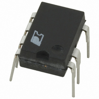
PKS604PN Power Integrations, PKS604PN Datasheet - Page 10

PKS604PN
Manufacturer Part Number
PKS604PN
Description
IC OFFLINE SWIT OTP OCP HV 8DIP
Manufacturer
Power Integrations
Series
PeakSwitch®r
Specifications of PKS604PN
Mfg Application Notes
PeakSwitch Design Guide AppNote
Output Isolation
Isolated
Frequency Range
250 ~ 304kHz
Voltage - Output
700V
Power (watts)
56W
Operating Temperature
-40°C ~ 150°C
Package / Case
8-DIP (0.300", 7.62mm), 7 Leads
Output Voltage
12 V
Input / Supply Voltage (max)
265 VAC
Input / Supply Voltage (min)
85 VAC
Duty Cycle (max)
65 %
Switching Frequency
47 KHz
Supply Current
25 uA
Operating Temperature Range
- 40 C to + 150 C
Mounting Style
Through Hole
For Use With
596-1126 - KIT DESIGN ACC PEAKSWITCH FAMILY
Lead Free Status / RoHS Status
Lead free / RoHS Compliant
Other names
596-1117-5
Available stocks
Company
Part Number
Manufacturer
Quantity
Price
Company:
Part Number:
PKS604PN
Manufacturer:
POWER
Quantity:
15 000
Part Number:
PKS604PN
Manufacturer:
POWER
Quantity:
20 000
Figure 14. Transformer Secondary Design Parameters Section of Spreadsheet – Multiple Outputs.
Step 7 – Selection of PeakSwitch External
Components
Bypass Pin Capacitor
For the BYPASS pin, use a 0.33 µF, 50 V ceramic capacitor or
a 1 µF, 50 V electrolytic, whichever is lower cost.
Step 8 – Selection of Under-Voltage or AC Line Sense
Components
UVLO prevents the supply from starting up prematurely, while
latching shutdown protects the IC, the supply and the load from
fault conditions. The rectified AC input voltage that forces the
current into the EN/UV pin to exceed 25 µA sets the UVLO
threshold.
Rev. E 02/07
TRANSFORMER SECONDARY DESIGN PARAMETERS (MULTIPLE OUTPUTS)
1st output
VO1
IO1
PO1
VD1
NS1
ISRMS1
IRIPPLE1
PIVS1
Recommended Diodes
CMS1
AWGS1
DIAS1
ODS1
2nd output
VO2
IO2
PO2
VD2
NS2
ISRMS2
IRIPPLE2
PIVS2
Recommended Diode
CMS2
AWGS2
DIAS2
ODS2
3rd output
VO3
IO3
PO3
VD3
NS3
ISRMS3
IRIPPLE3
PIVS3
Recommended Diode
CMS3
AWGS3
DIAS3
ODS3
Total power
Negative Output
10
AN-41
N/A
N/A
N/A
N/A
BYV27-
200
N/A
N/A
N/A
18.00 Watts
1.744 Amps
0.000 Amps
0.000 Amps
0.750 Amps
16.00
0.00 Watts
0.00 Watts
1.57 Amps
0.51 mm
0.49 mm
0.45
0.00 Amps
0.45
0.00 Amps
108 Volts
349 Cmils
0.7 Volts
0.7 Volts
0.7 Volts
18 Watts
24 Volts
24 AWG
2 Volts
0 Cmils
2 Volts
0 Cmils
Volts
Amps
AWG
mm
mm
Volts
Amps
AWG
mm
mm
For example, if regulation is lost due to a short circuit, an open
loop or an output overload condition, and the input voltage is
sufficient to support normal operation (>25 µA into the EN/UV
pin), then PeakSwitch will latch off. To reset the latch, the AC
input has to be removed long enough so that the current into
the EN/UV pin falls below the 25 µA UV threshold. Once
AC is reapplied, the next time the EN/UV pin current exceeds
25 µA, the supply will attempt to restart.
For some applications, the time for the EN/UV pin current to
fall below 25 µA may be excessive due to the time for the bulk
input capacitor to discharge. In such cases, a fast AC reset circuit
can be used allowing latching shutdown to be independent of
the load and voltage on the bulk input capacitor. This prevents
Main Output Voltage (if unused, defaults to single output design)
Output DC Current
Output Power
Output Diode Forward Voltage Drop
Output Winding Number of Turns
Output Winding RMS Current
Output Capacitor RMS Ripple Current
Output Rectifier Maximum Peak Inverse Voltage
Recommended Diodes for this output
Output Winding Bare Conductor minimum circular mils
Wire Gauge (Rounded up to next larger standard AWG value)
Minimum Bare Conductor Diameter
Maximum Outside Diameter for Triple Insulated Wire
Output Voltage
Output DC Current
Output Power
Output Diode Forward Voltage Drop
Output Winding Number of Turns
Output Winding RMS Current
Output Capacitor RMS Ripple Current
Output Rectifier Maximum Peak Inverse Voltage
Recommended Diodes for this output
Output Winding Bare Conductor minimum circular mils
Wire Gauge (Rounded up to next larger standard AWG value)
Minimum Bare Conductor Diameter
Maximum Outside Diameter for Triple Insulated Wire
Total Output Power
If negative output exists enter Output number; eg: If VO2 is
negative output, enter 2
Output Voltage
Output DC Current
Output Power
Output Diode Forward Voltage Drop
Output Winding Number of Turns
Output Winding RMS Current
Output Capacitor RMS Ripple Current
Output Rectifier Maximum Peak Inverse Voltage
Recommended Diodes for this output
Output Winding Bare Conductor minimum circular mils
Wire Gauge (Rounded up to next larger standard AWG value)
Minimum Bare Conductor Diameter
Maximum Outside Diameter for Triple Insulated Wire


