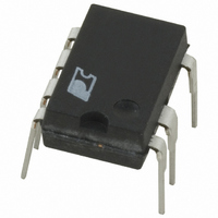
PKS604PN Power Integrations, PKS604PN Datasheet - Page 4

PKS604PN
Manufacturer Part Number
PKS604PN
Description
IC OFFLINE SWIT OTP OCP HV 8DIP
Manufacturer
Power Integrations
Series
PeakSwitch®r
Specifications of PKS604PN
Mfg Application Notes
PeakSwitch Design Guide AppNote
Output Isolation
Isolated
Frequency Range
250 ~ 304kHz
Voltage - Output
700V
Power (watts)
56W
Operating Temperature
-40°C ~ 150°C
Package / Case
8-DIP (0.300", 7.62mm), 7 Leads
Output Voltage
12 V
Input / Supply Voltage (max)
265 VAC
Input / Supply Voltage (min)
85 VAC
Duty Cycle (max)
65 %
Switching Frequency
47 KHz
Supply Current
25 uA
Operating Temperature Range
- 40 C to + 150 C
Mounting Style
Through Hole
For Use With
596-1126 - KIT DESIGN ACC PEAKSWITCH FAMILY
Lead Free Status / RoHS Status
Lead free / RoHS Compliant
Other names
596-1117-5
Available stocks
Company
Part Number
Manufacturer
Quantity
Price
Company:
Part Number:
PKS604PN
Manufacturer:
POWER
Quantity:
15 000
Part Number:
PKS604PN
Manufacturer:
POWER
Quantity:
20 000
Line Frequency, f
47 Hz for universal or 100/115 VAC input. 47 Hz for single
230 VAC input. For half-wave rectification use f
input enter the voltage directly into Cells B55 and B56.
Nominal Output Voltage, V
Enter the nominal output voltage of the main output during the
continuous load condition. Generally, the main output is the
output from which feedback is derived.
Output Current, I
Enter the maximum output current under peak load conditions.
If the design does not have a peak load condition, then enter
the maximum continuous output current. In multiple output
designs, the output current of the main output (typically, the
output from which feedback is taken) should be increased
such that the peak power (or maximum continuous power as
applicable) matches the sum of the output powers from all of the
supply’s outputs. The individual output voltages and currents
should then be entered at the bottom of the spreadsheet [cells
B98 to B131].
Minimum Output Voltage at Peak Load (V)
The output voltage may be specified in PeakSwitch designs based
on whether or not the output voltage is allowed to droop during
peak loads. If the application requires the output to remain the
same under continuous and peak load conditions, leave this cell
empty. The spreadsheet then assumes that the output voltage
under peak load conditions is equal to the nominal output voltage,
i.e. the output is not allowed to droop under peak load.
If the application allows the output voltage to droop under peak
load conditions, enter the minimum acceptable voltage at peak
load. The peak power is then calculated based on the output
current and the minimum acceptable output voltage. In multiple
output designs, if the main output is allowed to droop then all
the other output voltages will also droop proportionally under
peak load conditions.
Continuous Output Power (W)
Enter the continuous output power. If this entry is left blank the
design spreadsheet assumes that the continuous power is equal
to the peak output power. This value is used by the spreadsheet
to suggest a core size.
Peak Power (W)
This is a calculated value based on the minimum output voltage
at peak load, and maximum output current. It is used to calculate
the required value of the primary inductance.
Power Supply Efficiency, h
Enter the estimated efficiency of the complete power supply,
measured at the output terminals under peak load conditions
and worst-case line (generally lowest input voltage). Start
Rev. E 02/07
4
AN-41
L
O
(A)
O
(V)
L
/2. For DC
with a value of 0.7 (typical) for a design where the majority
of the output power is drawn from an output voltage of 12 V
or greater, and no current sensing is present on the secondary.
Once a prototype has been constructed, the measured efficiency
should be entered and the design of the transformer should be
iterated.
Power Supply Loss Allocation Factor, Z
This factor represents the proportion of losses between the
primary and the secondary of the power supply. Z factor is
used together with the efficiency number, to determine the
actual power that must be delivered by the power stage. For
example, losses in the input stage (EMI filter, rectification, etc)
are not processed by the power stage (transferred through the
transformer), and therefore, although they reduce efficiency,
the transformer design is not impacted.
For designs that do not have a secondary current sense circuit,
enter 0.65. For those designs that do have a secondary current
sense circuit, use a value of 0.7 until measurements can be made
on a prototype. The higher number indicates larger secondary
side losses associated with the secondary side current sense
resistor.
Bridge Diode Conduction Time, t
Enter a bridge diode conduction time of 3.75 ms, if there is no
better data available.
Total Input Capacitance, C
Enter the total input capacitance, using Table 3 for guidance.
Table 3. Suggested Total Input Capacitance for Different Input
The capacitance is used to calculate the minimum DC voltage
and should be selected to keep the minimum DC input voltage
(V
For designs that have a DC rather than an AC input, the value
of the minimum and maximum DC input voltages, V
V
design spreadsheet shown below.
AC Input Voltage
MAX
MIN
, may be entered directly into the override cells on the
) >70 V.
100/115
85-265
(VAC)
Voltage Ranges.
230
Total Input Capacitance per
Watt Output Power (µF/W)
IN
(µF)
Rectification
C
Full Wave
(ms)
3
1
3
MIN
and


