PKS604PN Power Integrations, PKS604PN Datasheet - Page 13
PKS604PN
Manufacturer Part Number
PKS604PN
Description
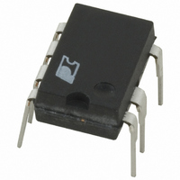
IC OFFLINE SWIT OTP OCP HV 8DIP
Manufacturer
Power Integrations
Series
PeakSwitch®r
Specifications of PKS604PN
Mfg Application Notes
PeakSwitch Design Guide AppNote
Output Isolation
Isolated
Frequency Range
250 ~ 304kHz
Voltage - Output
700V
Power (watts)
56W
Operating Temperature
-40°C ~ 150°C
Package / Case
8-DIP (0.300", 7.62mm), 7 Leads
Output Voltage
12 V
Input / Supply Voltage (max)
265 VAC
Input / Supply Voltage (min)
85 VAC
Duty Cycle (max)
65 %
Switching Frequency
47 KHz
Supply Current
25 uA
Operating Temperature Range
- 40 C to + 150 C
Mounting Style
Through Hole
For Use With
596-1126 - KIT DESIGN ACC PEAKSWITCH FAMILY
Lead Free Status / RoHS Status
Lead free / RoHS Compliant
Other names
596-1117-5
Available stocks
Company
Part Number
Manufacturer
Quantity
Price
Company:

Part Number:
PKS604PN
Manufacturer:
POWER
Quantity:
15 000
Part Number:
PKS604PN
Manufacturer:
POWER
Quantity:
20 000


Many capacitor manufacturers provide factors that increase
the ripple current rating as the capacitor operating temperature
is reduced from its data sheet maximum value. This should
be considered in order to ensure that the capacitor is not
oversized.
ESR Specification
The switching ripple voltage is equal to the peak secondary
current multiplied by the ESR of the output capacitor. It is
therefore important to select low ESR capacitors to reduce the
ripple voltage. In general, selecting a high ripple current rated
capacitor results in an acceptable value of ESR.
Voltage Rating
Select a voltage rating such that V
Step 12 – Select Feedback Circuit Components
The feedback loop is arranged to draw the disable current
(240 µA) from the EN/UV pin when the output voltage
reaches regulation. Ideally, the feedback loop should be able
to respond to the ripple on the output capacitor cycle-by-cycle.
Table 6. Example of Reference IC Feedback Configuration.
Voltage (V)
Output
12
18
24
30
5
8
Feedback Bias
Resistor, R
(kW)
1
BIAS
RATED
C
Opto Series
OUT
≥1.25 V
Resistor,
R
FB1
160
430
470
510
27
91
U
(W)
FB1
R
O
FB1
.
TL431
U
FB2
C
Capacitor,
Feedback
C
FB2
FB1
330
150
100
100
100
47
R
C
(nF)
BIAS
FB1
Due to the high switching frequency, a high gain optocoupler
of 300-600% is recommended to minimize feedback delay.
Adding a capacitor across the DC gain setting resistor (R12 in
Figure 1) further increases high frequency gain.
Table 5 shows a typical implementation of Zener feedback. The
series drops across D
LED U
depending on the availability of a suitable zener voltage. Resistor
R
close to its knee voltage. Resistor R
feedback. Both resistors can be 0.125 W or 0.25 W, 5%. To
increase high frequency gain, a ceramic capacitor C
across R
will minimize the current needed to bias the feedback network,
reducing no-load input power consumption.
Table 6 shows a typical implementation using a reference
IC for improved accuracy. Reference U
output voltage, programmed via the resistor divider R
Resistor R
while R
L
BIAS
PF
Capacitor,
Feedback
C
provides a 1 mA bias current so that VR
R
R
FB1
FB2
S1
S2
FB1
100
FB
determine the output voltage. Diode D
BIAS
. Selecting a Zener with a low test current (5 mA)
(nF)
sets the DC gain. Capacitor C
provides the minimum operating current for U
PI-4339-060706
C
Series Resistor
1, R
FB
PF
, VR
+V
RTN
S1
OUT
22.1
38.3
86.6
102
110
(kW) 1%
FB
10
, R
FB1
and the forward drop of the
FB1
AN-41
sets the DC gain of the
FB2
Sense Resistor
FB2
2, R
is used to set the
rolls off the gain
S1
FB
FB
(kW) 1%
10
is operating
FB1
is optional,
S1
is placed
and R
Rev. E 02/07
13
FB2
S2
.
Related parts for PKS604PN
Image
Part Number
Description
Manufacturer
Datasheet
Request
R

Part Number:
Description:
SOP-16
Manufacturer:
Power Integrations
Datasheet:
Part Number:
Description:
DIP8
Manufacturer:
Power Integrations
Datasheet:
Part Number:
Description:
TO-263
Manufacturer:
Power Integrations
Datasheet:
Part Number:
Description:
TO-263
Manufacturer:
Power Integrations
Datasheet:
Part Number:
Description:
Manufacturer:
Power Integrations
Datasheet: