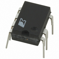
PKS604PN Power Integrations, PKS604PN Datasheet - Page 7

PKS604PN
Manufacturer Part Number
PKS604PN
Description
IC OFFLINE SWIT OTP OCP HV 8DIP
Manufacturer
Power Integrations
Series
PeakSwitch®r
Specifications of PKS604PN
Mfg Application Notes
PeakSwitch Design Guide AppNote
Output Isolation
Isolated
Frequency Range
250 ~ 304kHz
Voltage - Output
700V
Power (watts)
56W
Operating Temperature
-40°C ~ 150°C
Package / Case
8-DIP (0.300", 7.62mm), 7 Leads
Output Voltage
12 V
Input / Supply Voltage (max)
265 VAC
Input / Supply Voltage (min)
85 VAC
Duty Cycle (max)
65 %
Switching Frequency
47 KHz
Supply Current
25 uA
Operating Temperature Range
- 40 C to + 150 C
Mounting Style
Through Hole
For Use With
596-1126 - KIT DESIGN ACC PEAKSWITCH FAMILY
Lead Free Status / RoHS Status
Lead free / RoHS Compliant
Other names
596-1117-5
Available stocks
Company
Part Number
Manufacturer
Quantity
Price
Company:
Part Number:
PKS604PN
Manufacturer:
POWER
Quantity:
15 000
Part Number:
PKS604PN
Manufacturer:
POWER
Quantity:
20 000
Figure 8 provides an illustration of the difference between
transient and steady state K
waveforms for a design that does not meet K
limits.
In region (a) the K
the control loop has caused a switching cycle to be skipped,
allowing the flux in the transformer core to be completely
reset as the output diode is allowed to conduct for a much
longer duration than in region (a). On the next switching cycle
(c), the feedback loop has enabled a switching pulse and the
current ramps from zero rather than some initial value. This
means that the on-time for switching cycle (c) is much longer
than for (a), allowing less off-time (the time during which the
output diode conducts), yielding less resetting of the core flux.
Therefore, cycle (d) starts with a much larger initial current
pedestal than during the steady state conditions of (a). In the
following cycles, (e) and (f), the value of K
the K
The sequence of skipped cycle (b) followed by a cycle
that gives the minimum possible off time (c) is where the
spreadsheet calculates the value of K
K
To address this problem a larger device could be selected, the
V
K
initial current pedestal from falsely triggering current limit at
the end of the leading edge blanking time and limiting power
delivery. Similar guidance is given in the comment cell on
how to maintain K
Figure 8. Drain Current Waveform Illustrating K
Figure 9. Under-Voltage Variables Section of Design Spreadsheet.
Figure 10. Bias Winding Variables Section of Design Spreadsheet.
ENTER UVLO VARIABLES
V_UV_TARGET
V_UV_ACTUAL
RUV_IDEAL
RUV_ACTUAL
BIAS WINDING VARIABLES
VB
NB
PIVB
P (TRANSIENT)
OR
P (TRANSIENT)
I
I
K
increased, or the output power reduced.
R
P
P
P (STEADY STATE)
= 0.3 A
= 0.8 A
= 0.38
Drain Current
Secondary (Diode) Current
Skipped Cycle
(a)
is 0.19, below the 0.25 limit and is thus unacceptable.
should be above a value of 0.25 to prevent the large
P
of 0.38.
P (TRANSIENT)
is stable with a value of 0.38. In region (b)
I
I
K
R
P
P
= 0.3 A
= 0.8 A
= 0.38
P
. It shows a series of drain current
within acceptable limits.
P (TRANSIENT)
(b)
P(STEADY STATE)
P
. In this example,
settles again to
P (TRANSIENT)
and K
(c)
I
I
K
R
P
P(TRANSIENT)
P
= 0.8 A
= 0.8 A
15.00 Volts
= 1
3.45 Mohms
3.30 Mohms
88 Volts
85 Volts
10
68 Volts
Step 3 – Enter Under-Voltage Lock Out (UVLO)
Variables, V
The line under-voltage lockout feature of PeakSwitch sets the
minimum startup voltage of the supply, prevents the power
supply output from glitching when the input voltage is below
the normal operating range, and is used to determine if the
supply should latch off during a fault. Connecting a resistor
from an input capacitor to the EN/UV pin enables this feature.
Enter the desired DC voltage across the input capacitor, at
which the power supply should start operating. The spreadsheet
calculates both the ideal resistor value and closest standard value,
together with the typical start-up voltage based on the closest
standard value (Figure 9). Either a resistor with a voltage rating
>375 V or two series resistors whose voltage rating sum is
>375 V should be used.
Step 4 – Choose Bias Winding Output Voltage, V
By default, if the grey override cell is left empty, a value
of 15 V is assumed. The user can override this value as
needed. However, the value should be in the range of 8 V <V
<20 V. The lower value ensures adequate headroom for supplying
current into the BYPASS pin. The upper value limits the no-load
input power consumption caused by high power consumption
in the bias winding. The number of bias winding turns, N
is to be used for transformer construction. An ultra-fast diode
with a voltage rating above the calculated PIVB value should
be selected. Select the value of resistor from the bias supply
to the BYPASS pin to provide the maximum data sheet supply
current for the selected PeakSwitch device.
I
I
K
R
P
.
P
(d)
= 0.8 A
= 0.15 A
= 0.19
Target DC under-voltage threshold, above which the power
supply with start
Typical DC start-up voltage based on standard value of
RUV_ACTUAL
Calculated value for UV Lockout resistor
Closest standard value of resistor to RUV_IDEAL
Bias winding Voltage
Number of Bias Winding Turns
Bias rectifier Maximum Peak Inverse Voltage
_UV_TARGET
(e)
I
I
K
R
P
P
= 0.38 A
= 0.8 A
= 0.48
(V)
I
I
K
R
P
P
= 0.8 A
= 0.28 A
= 0.35
AN-41
PI-4337-031706
(f)
I
I
K
R
P
P
= 0.3 A
= 0.8 A
= 0.38
Rev. E 02/07
B
7
(V)
B
B
,


