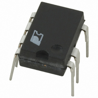
PKS604PN Power Integrations, PKS604PN Datasheet - Page 5

PKS604PN
Manufacturer Part Number
PKS604PN
Description
IC OFFLINE SWIT OTP OCP HV 8DIP
Manufacturer
Power Integrations
Series
PeakSwitch®r
Specifications of PKS604PN
Mfg Application Notes
PeakSwitch Design Guide AppNote
Output Isolation
Isolated
Frequency Range
250 ~ 304kHz
Voltage - Output
700V
Power (watts)
56W
Operating Temperature
-40°C ~ 150°C
Package / Case
8-DIP (0.300", 7.62mm), 7 Leads
Output Voltage
12 V
Input / Supply Voltage (max)
265 VAC
Input / Supply Voltage (min)
85 VAC
Duty Cycle (max)
65 %
Switching Frequency
47 KHz
Supply Current
25 uA
Operating Temperature Range
- 40 C to + 150 C
Mounting Style
Through Hole
For Use With
596-1126 - KIT DESIGN ACC PEAKSWITCH FAMILY
Lead Free Status / RoHS Status
Lead free / RoHS Compliant
Other names
596-1117-5
Available stocks
Company
Part Number
Manufacturer
Quantity
Price
Company:
Part Number:
PKS604PN
Manufacturer:
POWER
Quantity:
15 000
Part Number:
PKS604PN
Manufacturer:
POWER
Quantity:
20 000
Figure 4. DC Input Voltage Parameters Showing Grey Override Cells for DC Input Designs.
Step 2 – Enter PeakSwitch Variables: PeakSwitch
Device, V
Select the correct PeakSwitch device
Refer to Table 1 and first select a device based on the peak
output power of the design. Then compare the continuous
power rating to the continuous numbers in the power table.
If the continuous power exceeds the value given in the power
table, then the next largest device should be selected. Similarly,
if the continuous power is close to the power table’s power
levels, then it may be necessary to switch to a larger device
based on the measured thermal performance of the prototype.
Figure 5. PeakSwitch Section of Design Spreadsheet.
Peak Load Switching Frequency, f
This parameter is the worst-case minimum switching
frequency based on the minimum data sheet value of I
adjustable).
Reflected Output Voltage, V
This parameter is the secondary winding voltage during the
diode conduction time, which is reflected back to the primary
through the turns ratio of the transformer. The default value
is 110 V, however the acceptable range for V
80 V and 135 V, providing that no warnings are produced by the
spreadsheet. For design optimization purposes, the following
should be kept in mind:
1. Higher V
2. Higher V
ENTER PeakSwitch VARIABLES
PeakSwitch
Chosen Device
ILIMITMIN
ILIMITMAX
fSmin
I^2fmin
VOR
VDS
VD
VDB
VCLO
KP (STEADY STATE)
KP (TRANSIENT)
DC INPUT VOLTAGE PARAMETERS
VMIN
VMAX
minimizes the value of the input capacitor and the droop of
the output voltage when the on-time extension feature is used,
and maximizes the power delivery from a given PeakSwitch
device.
which in some cases may allow a Schottky diode to be used,
and will thus give higher efficiency.
OR
OR
OR
, V
allows increased power delivery at V
reduces the voltage stress on the output diodes,
DS
, V
D
, V
DB
, V
CLO
OR
, K
(V)
PKS603P
P(STEADY STATE)
s(min)
(Hz)
OR
, K
PKS603P
is between
P(TRANSIENT)
MIN
, which
2
f (not
PKS603P
250000 Hertz
0.750 Amps
0.870 Amps
0.60
0.38
164 A^2kHz
110 Volts
200 Volts
375 Volts
0.7 Volts
0.7 Volts
10 Volts
80 Volts
3. Higher V
4. Higher V
Optimal selection of the V
reasonable engineering compromise of the factors mentioned
above.
PeakSwitch On-State Drain to Source Voltage, V
This parameter is the average on-state voltage developed across
the DRAIN and SOURCE pins of the PeakSwitch device. By
default, if the grey override cell is left empty, a value of 10 V
is assumed for Y/F package devices, and 5 V for P package
devices. Use the default value if no better data is available.
Output Diode Forward Voltage Drop, V
Enter the average forward voltage drop of the (main) output
diode. Use 0.5 V for a Schottky diode or 0.7 V for a PN diode,
if no better data is available. The spreadsheet uses a default
value of 0.7 V.
Nominal Clamp Voltage, V
Enter the nominal clamp voltage. The clamp is used to ensure
that maximum voltage developed across the DRAIN and
SOURCE pins of the internal MOSFET remains below the
BV
recommended that a Zener diode with a value of 200 V be used
in the clamp circuit. Even if an RCD clamp is used, a Zener
should be placed in parallel with the RCD circuit to provide
hard clamping during fault conditions. By default, if the grey
override cell is left empty, a value of 200 V is assumed, which
is also the maximum value recommended. Lower values can
which reduces efficiency of the power supply.
secondary side, which may increase secondary side copper
and diode losses.
DSS
specification (700 V) limit, with sufficient margin. It is
Minimum DC Input Voltage
Maximum DC Input Voltage
PeakSwitch device
Minimum Current Limit
Maximum Current Limit
Minimum Device Switching Frequency
I^2f (product of current limit squared and frequency is trimmed
for tighter tolerance)
Reflected Output Voltage (VOR <= 135 V Recommended)
PeakSwitch on-state Drain to Source Voltage
Output Winding Diode Forward Voltage Drop
Bias Winding Diode Forward Voltage Drop
Nominal Clamp Voltage
Ripple to Peak Current Ratio (KP < 6)
Ripple to Peak Current Ratio under worst case at peak load
(0.25 < KP < 6)
OR
OR
increases the leakage inductance of the transformer,
increases the peak and RMS currents on the
CLO
OR
value should be based on a
(V)
AN-41
D
(V)
DS
(V)
Rev. E 02/07
5


