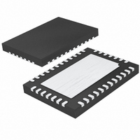
LTC4245CUHF#PBF Linear Technology, LTC4245CUHF#PBF Datasheet - Page 10

LTC4245CUHF#PBF
Manufacturer Part Number
LTC4245CUHF#PBF
Description
IC CNTRLR HOT SWAP 38-QFN
Manufacturer
Linear Technology
Type
Hot-Swap Controllerr
Datasheet
1.LTC4245CUHFPBF.pdf
(36 pages)
Specifications of LTC4245CUHF#PBF
Applications
CompactPCI™
Internal Switch(s)
No
Voltage - Supply
3.3V, 5V, 12V
Operating Temperature
0°C ~ 70°C
Mounting Type
Surface Mount
Package / Case
38-WFQFN, Exposed Pad
Family Name
LTC4245
Package Type
QFN EP
Operating Supply Voltage (min)
2.25/4.25/10.2/-10.2V
Operating Supply Voltage (max)
0/10/20/-20V
Operating Temperature (min)
0C
Operating Temperature (max)
70C
Operating Temperature Classification
Commercial
Product Depth (mm)
5mm
Product Length (mm)
7mm
Mounting
Surface Mount
Pin Count
38
Lead Free Status / RoHS Status
Lead free / RoHS Compliant
Available stocks
Company
Part Number
Manufacturer
Quantity
Price
PI FU CTIO S
LTC4245
5V
Bad Input. Connect this pin to the source of the 5V supply
external N-channel MOSFET switch for gate drive return.
Power is considered bad if this pin drops below 4.63V or
2.9V depending on the CFG pin. The comparator on this
pin has a built-in hysteresis of 17mV or 11mV. This pin
is also an input to the ADC and the current limit foldback
circuit. A 180Ω active pull-down discharges 5V
ground when the external MOSFET is turned off.
5V
nect this pin to the output of the 5V current sense resistor.
The current limit circuit controls the 5V
the sense voltage between the 5V
25mV or less during start-up and 75mV thereafter. Dur-
ing start-up a foldback feature reduces the current limit
to 7.5mV as the 5V
breaker, enabled after start-up, trips when the sense voltage
exceeds 25mV for 22μs. To disable current limit, connect
this pin to 5V
ADR0 to ADR3: Serial Bus Address Inputs. ADR0 and
ADR1 are two-state inputs; ADR2 and ADR3 are three-
state inputs. Tying these pins to ground, open or INTV
confi gures one of 32 possible addresses. The addressing
scheme is compatible with the CompactPCI geographic
addressing for slot identifi cation. See Table 5 in Applica-
tions Information.
ALERT#: Fault Alert Output. Open-drain logic output that can
be pulled to ground, when a fault occurs, to alert the host
controller. A fault alert is enabled by the ALERT register.
This device is compatible with SMBus alert protocol. See
Applications Information. Tie to ground if unused.
BD_SEL#: Board Present Input. Ground this pin to enable
the N-channel MOSFETs to turn on. When this pin is high,
the MOSFETs are off. An internal 10μA current source
pulls up this pin to INTV
recorded in the FAULT2 register. A high-to-low transition
activates the logic to read the state of the ON pin and clear
faults. See Applications Information.
CFG: Supply Confi guration Three-State Input. When this
pin is grounded, all four supply inputs must satisfy their
undervoltage lockout levels to allow the external MOSFETs
10
OUT
SENSE
U
: 5V Gate Drive Return; Foldback, ADC and Power
: 5V Supply Current Sense and ADC Input. Con-
U
IN
.
OUT
U
pin approaches ground. A circuit
CC
. Transitions on this pin will be
IN
and 5V
GATE
SENSE
pin to limit
pins to
OUT
CC
to
to turn on. Floating this pin disables V
lockout and power bad functions, allowing other supplies
to turn-on even when –12V supply is absent. Tying this
pin to INTV
the 5V
levels. This allows using an extra 3.3V supply instead of
a 5V supply as in a PCI Express application.
EXPOSED PAD (Pin 39, UHF Package): Exposed Pad may
be left open or connected to device ground.
GND: Device Ground.
GPIO1 to GPIO3 (GPIO2, GPIO3 on UHF package only):
General Purpose Input/Output and ADC Input. Open-drain
logic outputs and logic inputs. Any one of the three pins
can be multiplexed to the GPIO channel of the internal
ADC. GPIO1 has a state change fault associated with it.
The GPIO register (Table 13) contains status and control
bits for these pins.
HEALTHY#: Board Power Status Output. This pin is pulled
low by an open-drain output when all supply outputs are
above their power bad thresholds and when all external
N-channel MOSFETs are on. When any supply output
falls below its power bad threshold voltage, this pin will
go high after a 15μs deglitching time.
INTV
Connect a 0.1μF capacitor from this pin to ground. When
this pin falls below 3.8V, the internal registers are reset.
LOCAL_PCI_RST#: Reset Output. This pin is pulled low by
an open-drain output whenever HEALTHY# is high or when
the PCI_RST# input is low. Tie to ground if unused.
ON: On Control Input. A rising edge turns on the external
N-channel MOSFETs and a falling edge turns them off.
This pin is also used to confi gure the state of the FET On
control bits (and hence the external FETs) in the ON regis-
ter. For example, if the ON pin is tied high, then one or all
(depending on the Sequence control bit) FET On control
bits will go high 100ms after power-up. Likewise if the ON
pin is tied low then the part will remain off after power-up
until the FET On control bits are set high using the I
bus. If the Sequence control bit is set, taking ON pin high
turns on the supplies in a 12V, 5V, 3.3V, –12V sequence.
A high-to-low transition on this pin will clear faults.
CC
IN
: Internal Low Voltage Supply Decoupling Output.
undervoltage, power bad and ADC levels to 3.3V
CC
not only disables V
EE
, but also converts
EE
undervoltage
4245fa
2
C


