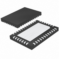
LTC4245CUHF#PBF Linear Technology, LTC4245CUHF#PBF Datasheet - Page 16

LTC4245CUHF#PBF
Manufacturer Part Number
LTC4245CUHF#PBF
Description
IC CNTRLR HOT SWAP 38-QFN
Manufacturer
Linear Technology
Type
Hot-Swap Controllerr
Datasheet
1.LTC4245CUHFPBF.pdf
(36 pages)
Specifications of LTC4245CUHF#PBF
Applications
CompactPCI™
Internal Switch(s)
No
Voltage - Supply
3.3V, 5V, 12V
Operating Temperature
0°C ~ 70°C
Mounting Type
Surface Mount
Package / Case
38-WFQFN, Exposed Pad
Family Name
LTC4245
Package Type
QFN EP
Operating Supply Voltage (min)
2.25/4.25/10.2/-10.2V
Operating Supply Voltage (max)
0/10/20/-20V
Operating Temperature (min)
0C
Operating Temperature (max)
70C
Operating Temperature Classification
Commercial
Product Depth (mm)
5mm
Product Length (mm)
7mm
Mounting
Surface Mount
Pin Count
38
Lead Free Status / RoHS Status
Lead free / RoHS Compliant
Available stocks
Company
Part Number
Manufacturer
Quantity
Price
APPLICATIO S I FOR ATIO
LTC4245
When a switch is to be turned on, an internal 100μA cur-
rent source is connected to the TIMER pin and a 20μA
current to SS pin. The gate of each ramping supply’s pass
transistor is servoed by an internal amplifi er, so the supply
current never exceeds an internal current limit. This internal
current limit starts off with a negative value, which makes
the amplifi er pull the gate low. The voltage ramp on the
SS pin is converted to a current limit rising linearly with
time. The amplifi er releases the gate as the current limit
crosses zero. An internal current source starts charging
up the gate. When the gate voltage reaches the MOSFET
threshold voltage, the switch begins to turn on. The
amplifi er once again starts modulating the gate pull-up
current so that the sense resistor voltage drop follows the
internally set current limit. The rate of rise of the inrush
current is given by:
G
in SS pin voltage. The rising current limit will stop at a
level depending on the foldback circuit. The foldback circuit
monitors the outputs of all supplies which are ramping.
In the worst case, a supply output could be shorted to
ground. In this case the foldback circuit reduces the cur-
rent limit to 30% of the maximum as shown in the Typical
Performance Curves. To set an inrush current lower than
the foldback level, a series R-C network can be connected
between the gate pin and ground (V
(Figure 3). This allows charging the output load beyond
the time dictated by the TIMER capacitor. When the rising
internal current limit exceeds the dV/dt set inrush current,
the current limit amplifi er goes open loop. If any ramping
supply’s amplifi er is open loop the SS pin current drops
to 2μA from 20μA, thus slowing the current limit rise.
This would affect the other supplies ramp-up in case of
simultaneous turn-on. A 100kΩ resistance ensures that
the capacitor charge is decoupled during a fast gate turn-
off. The capacitor value is determined by:
16
SS
C
dI
dV
is the ratio of the change in current limit to the change
GATE
dt
INRUSH
SS
dt
=
=
C
I
I
SS
GATE UP
I
=
SS
INRUSH
R
G
SENSE
(
SS
U
)
•
C
•
LOAD
dV
U
dt
SS
EEOUT
W
for –12V supply)
U
(1)
(2)
( 3 )
Meanwhile the TIMER pin ramps up to 2.56V, when it is
reset to ground. Current limit faults on the ramping supplies
are ignored during this time period. The start-up timing
cycle ends when the TIMER pin falls below 0.23V. The SS
pin is reset, the circuit breaker for the supply is armed and
its current limit raised to 3x the circuit breaker threshold.
In a sequenced turn-on the part will start another TIMER
and SS cycle to ramp up the next supply. If supplies are
being turned on through the serial bus, it will wait for the
next turn-on command.
Once all supplies have been turned on and all their outputs
are within tolerance, HEALTHY# will pull low and LO-
CAL_PCI_RST#, which was low, will now follow PCI_RST#.
The TIMER pin is now pulled up by a 10μA current source
while SS pin remains in reset. When TIMER reaches 2.56V,
it is reset to ground. As it crosses 0.23V the PGI pin is
sampled. If it is low then all switches are turned off.
3V
OUT
Figure 3. C
LOCAL_PCI_RST#
, V
*ADDITIONAL DETAILS
OMITTED FOR CLARITY
EEOUT
12V
Figure 2. Normal Turn-On Waveform
OUT
HEALTHY#
BD_SEL#
, 10V/DIV
2.5V/DIV
2.5V/DIV
, 5V
5V/DIV
5V/DIV
5V/DIV
TIMER
GATE
OUT
SS
for dV/dt Limited Inrush Current
Q2, Si7880DP
LTC4245G*
Q4, Si4872
V
17
5V
EEGATE
GATE
34
R6
10Ω
R8
10Ω
100k C
R27
TIME 50ms/DIV
GATE(VEE)
100k
R26
V
EEOUT
4245 F03
18
C
GATE(5V)
4245 F02
4245fa


