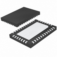
LTC4245CUHF#PBF Linear Technology, LTC4245CUHF#PBF Datasheet - Page 13

LTC4245CUHF#PBF
Manufacturer Part Number
LTC4245CUHF#PBF
Description
IC CNTRLR HOT SWAP 38-QFN
Manufacturer
Linear Technology
Type
Hot-Swap Controllerr
Datasheet
1.LTC4245CUHFPBF.pdf
(36 pages)
Specifications of LTC4245CUHF#PBF
Applications
CompactPCI™
Internal Switch(s)
No
Voltage - Supply
3.3V, 5V, 12V
Operating Temperature
0°C ~ 70°C
Mounting Type
Surface Mount
Package / Case
38-WFQFN, Exposed Pad
Family Name
LTC4245
Package Type
QFN EP
Operating Supply Voltage (min)
2.25/4.25/10.2/-10.2V
Operating Supply Voltage (max)
0/10/20/-20V
Operating Temperature (min)
0C
Operating Temperature (max)
70C
Operating Temperature Classification
Commercial
Product Depth (mm)
5mm
Product Length (mm)
7mm
Mounting
Surface Mount
Pin Count
38
Lead Free Status / RoHS Status
Lead free / RoHS Compliant
Available stocks
Company
Part Number
Manufacturer
Quantity
Price
OPERATIO
Start-Up
The LTC4245 is designed to turn a board’s supply voltages
on and off in a controlled manner, allowing the board to be
safely inserted or removed from a live backplane slot. When
a supply turn-on command is received, current sources
start pulling up the TIMER and SS pins. The 100μA I
current and the external TIMER capacitor determine the
time a supply can be in current limit during start-up. The
gate of a supply’s external N-channel MOSFET is servoed
by an amplifer (ACL
the sense resistor voltage drop, never exceeds an internal
current limit. This current limit rises at a rate determined
by I
determines the maximum value of the current limit and
reduces it to 30% of the maximum when a supply’s output
is shorted to ground. When the TIMER pin crosses 2.56V
it is reset to ground and the start-up timing cycle ends. If
a supply is still in current limit all gates are turned off, an
overcurrent fault is logged and the TIMER goes through
a cool-down timing cycle using 2μA for I
its circuit breaker (ECB
is raised to 3 times the circuit breaker threshold. The SS
pin is then reset by switch M2.
Any combination of the four supplies can be turned on
together or one after another. Whenever a supply is ramp-
ing up, its output voltage will affect, through the foldback
circuit, where the internal current limit ramp stops. The
default confi guration turns on all supplies together. If
sequence control bit C6 (Table 9) is set, the supplies turn
on in a 12V, 5V, 3.3V, –12V sequence. With this bit set,
the end of a supply ramp-up triggers the start of the next
one in the sequence. The I
on and off control for each supply through its On control
bit. Turn-off is simultaneous under fault conditions and
when using the ON or BD_SEL# pins.
At the end of the last start-up timing cycle, HEALTHY#
is pulled low by M3 if all supply outputs are above their
power bad thresholds. LOCAL_PCI_RST# which was held
low (M4), now follows PCI_RST#. The TIMER pin goes
through a PGI timeout cycle using 10μA for I
pin is sampled at the end of the cycle. If it is low, then
all external MOSFETs are shut-off, a PGI fault is logged
and TIMER goes through a cool-down cycle using 2μA
SS
and the capacitor at the SS pin. A foldback circuit
U
n
) so that the current, as indicated by
n
) is armed and the current limit
2
C interface allows independent
TMR
TMR
. Otherwise,
. The PGI
TMR
for I
of operation.
Normal Operation
During normal operation, the gates of the MOSFETs are
clamped about 6.2V above their sources. The 12V gate
driver uses a charge pump, the 5V and 3.3V gate drive is
derived from 12V
Each supply is continuously monitored for undervoltage,
overcurrent and power bad conditions. Overcurrent moni-
toring consists of an electronic circuit breaker comparator
(ECB
ECB threshold. Undervoltage and overcurrent faults cause
all MOSFETs to be shut off. A power bad condition causes
HEALTHY# to go high impedance and LOCAL_PCI_RST#
to pull low, without shutting off the MOSFETs. If the PGI
pin is not disabled (register bit C3 not set), then PGI pin
going low will also shut off all MOSFETs.
ADC
Included in the LTC4245 is an 8-bit A/D converter. The
converter has a 13-input multiplexer to select between
input, output and current sense voltage of each supply,
and the GPIO channel. The ADC can either cycle through
all channels or measure a channel on-demand.
Serial Interface
An I
status, control and A/D registers. It allows the host to poll
the device and determine if faults have occurred. If the
ALERT# line is used as an interrupt, the host can respond
to a fault in real time. The LTC4245 I
dress is decoded using the ADR0 to ADR3 pins.
Confi guration, GPIO and Precharge
The three-state CFG pin can be used to disable the V
undervoltage lockout, power bad and foldback functions.
It can also convert the 5V undervoltage, power bad and
ADC levels to 3.3V levels. The GPIO1 to GPIO3 pins can
be used as general purpose inputs or outputs (M5 to
M7). One of the pins can also be multiplexed to the GPIO
channel of the ADC. A 1V reference voltage derived from
3V
to pre-charge I/O lines on the board so as not to corrupt
the backplane bus.
IN
2
TMR
n
is provided at the PRECHARGE pin. This can be used
C interface is provided to read from or write to the
) and an active current limit circuit (ACL
. If PGI is high, the part enters the normal mode
IN
and the –12V gate drive from INTV
2
C interface slave ad-
LTC4245
n
) set at 3x the
13
4245fa
CC
EE
.


