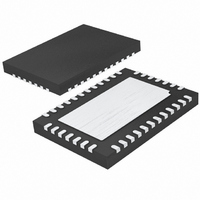
LTC4245CUHF#PBF Linear Technology, LTC4245CUHF#PBF Datasheet - Page 21

LTC4245CUHF#PBF
Manufacturer Part Number
LTC4245CUHF#PBF
Description
IC CNTRLR HOT SWAP 38-QFN
Manufacturer
Linear Technology
Type
Hot-Swap Controllerr
Datasheet
1.LTC4245CUHFPBF.pdf
(36 pages)
Specifications of LTC4245CUHF#PBF
Applications
CompactPCI™
Internal Switch(s)
No
Voltage - Supply
3.3V, 5V, 12V
Operating Temperature
0°C ~ 70°C
Mounting Type
Surface Mount
Package / Case
38-WFQFN, Exposed Pad
Family Name
LTC4245
Package Type
QFN EP
Operating Supply Voltage (min)
2.25/4.25/10.2/-10.2V
Operating Supply Voltage (max)
0/10/20/-20V
Operating Temperature (min)
0C
Operating Temperature (max)
70C
Operating Temperature Classification
Commercial
Product Depth (mm)
5mm
Product Length (mm)
7mm
Mounting
Surface Mount
Pin Count
38
Lead Free Status / RoHS Status
Lead free / RoHS Compliant
Available stocks
Company
Part Number
Manufacturer
Quantity
Price
APPLICATIO S I FOR ATIO
Resetting Faults
The two fault registers E and F can be reset in any of the
following ways:
Note that faults that are still present cannot be cleared.
Overcurrent and PGI faults are continuously set during their
cool-down timing cycles and hence cannot be reset for
that duration. The fault registers will not be cleared when
auto-retrying. When autoretry is disabled the existence of
an undervoltage (E0 to E3), overcurrent (E4 to E7) or PGI
(F4) fault keeps the switches off. As soon as the fault is
cleared, the switches will turn on.
1. Writing zeros to the registers using the I
2. Taking the ON pin high to low resets both
3. INTV
4. Bringing BD_SEL# from high to low clears all fault bits
I/O PIN 128
BD_SEL#
registers.
threshold.
except bit F6. Bit F6, which indicates a BD_SEL#
change of state, will be set.
LONG 5V
GROUND
I/O PIN 1
5V
CC
CONNECTOR
BACKPLANE
falling below its undervoltage lockout
Figure 10. Precharge Bus Switch Application Circuit for 3.3V and Universal Hot Swap Boards
U
CONNECTOR
CARD
U
Z2: SMAJ5.0A
*ADDITIONAL DETAILS OMITTED FOR CLARITY
DATA BUS
2.74Ω
W
C4
10nF
PER PIN
R18
C5
10nF
PER PIN
Z2
2
5V
U
C bus.
IN
51k 5%
R24
R17
1.2k
5%
R25
75k
5%
Q5
MMBT3906
100Ω
Precharge
The PRECHARGE pin provides a 1V voltage (using a divided
down 3V
bus connector pins during board insertion and extraction.
The pin can source 70mA without losing regulation. An
external 18Ω resistor from this pin to ground provides the
current sink capability. At least one long 3.3V connector
pin must be connected to 3V
the precharge circuit.
Resistors are used to connect the 1V bias voltage to the
CPCI bus signals. For 5V signaling this resistance must
be greater than 10kΩ - 5% (Figure 1). For 3.3V signaling
if the leakage current on the I/O line is greater than 2µA,
the precharge resistors need to be disconnected during
normal operation. Figure 10 shows a circuit that uses a
bus switch to accomplish this. The connection is made
when the voltage on the BD_SEL# pin is pulled up to 5V,
which occurs just after the long pins have made contact.
The resistors are disconnected when the short BD_SEL#
connector pin makes contact and the BD_SEL# voltage
drops below 4.4V thus causing ⎯ O ⎯ E to be pulled high by
10
36
0.1µF
10Ω
10Ω
R20
R21
5%
5%
5V
BD_SEL#
C10
IN
GND
IN
9
18Ω 5%
as the reference) that is used to bias the CPCI
R9
OE
PRECHARGE
OUT
V
BUS SWITCH
DD
R22
10k
5%
23
LTC4245G*
OUT
IN
UP TO 128 I/O LINES
R23
10k
5%
IN
to provide early power to
LTC4245
I/O
I/O
BRIDGE
CHIP
PCI
21
4245 F10
4245fa


