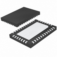
LTC4245CUHF#PBF Linear Technology, LTC4245CUHF#PBF Datasheet - Page 11

LTC4245CUHF#PBF
Manufacturer Part Number
LTC4245CUHF#PBF
Description
IC CNTRLR HOT SWAP 38-QFN
Manufacturer
Linear Technology
Type
Hot-Swap Controllerr
Datasheet
1.LTC4245CUHFPBF.pdf
(36 pages)
Specifications of LTC4245CUHF#PBF
Applications
CompactPCI™
Internal Switch(s)
No
Voltage - Supply
3.3V, 5V, 12V
Operating Temperature
0°C ~ 70°C
Mounting Type
Surface Mount
Package / Case
38-WFQFN, Exposed Pad
Family Name
LTC4245
Package Type
QFN EP
Operating Supply Voltage (min)
2.25/4.25/10.2/-10.2V
Operating Supply Voltage (max)
0/10/20/-20V
Operating Temperature (min)
0C
Operating Temperature (max)
70C
Operating Temperature Classification
Commercial
Product Depth (mm)
5mm
Product Length (mm)
7mm
Mounting
Surface Mount
Pin Count
38
Lead Free Status / RoHS Status
Lead free / RoHS Compliant
Available stocks
Company
Part Number
Manufacturer
Quantity
Price
PI FU CTIO S
PCI_RST#: Reset Input. Pulling this pin low causes LO-
CAL_PCI_RST# to pull low. When high, LOCAL_PCI_RST#
is the logical inverse of HEALTHY#. Tie to INTV
unused.
PGI: Power Good Input. Tie this pin to the ⎯ R ⎯ E ⎯ S ⎯ E ⎯ T output
of an external supply monitor or power good output of a
DC/DC converter. When all supplies have been turned on,
a timing cycle is started at the end of which the PGI pin is
sampled. If it is low, all external MOSFETs are shut off. If
the PGI Disable control bit C3 is not set, pulling this pin
low for more than 20μs during normal operation will also
shut off all MOSFETs. Tie to INTV
PRECHARGE: Bus Precharge Output. This pin can source
70mA at 1V as soon as 3V
if unused.
SCL: Serial Bus Clock Input. Data at the SDA pin is shifted
in or out on rising edges of SCL. This is a high impedance
pin that is generally driven by an open-collector output
from a master controller.
SDA: Serial Bus Data Input and Output. This is a high
impedance input when address, command or data bits
are shifted in. It is an open-drain output when sending
data back to the master controller or acknowledging a
write operation. An external pull-up resistor or current
source is required.
SS: Soft-Start Input. Connect a capacitor between this pin
and ground to set the rate of increase of current limit during
start-up for dI/dt limited inrush current. When an external
MOSFET is turned on, a 20μA pull-up current charges the
capacitor. The voltage ramp on the capacitor is converted
into an internal current limit increasing linearly with time.
Leave it open if dI/dt limited inrush is not required.
TIMER: Timer Input. A capacitor between this pin and
ground sets the duration of the start-up, PGI and auto-retry
timing cycles to be 23.3ms/μF, 233ms/μF and 1.17s/μF
respectively. A timing cycle consists of TIMER being
charged to 2.56V with an internal pull-up current source
and then being reset by a switch to ground. The timing
cycle ends when TIMER falls below 0.23V. The start-up,
PGI and auto-retry timing cycles use 100μA, 10μA and
2μA pull-up current sources respectively.
U
U
U
IN
is powered-up. Leave it open
CC
if unused.
CC
if
V
nel MOSFET. An internal 20μA current source charges
the gate of the external N-channel MOSFET. An internal
clamp limits the gate voltage to 6.2V above V
turn-off, a 3.5mA pull-down current discharges V
to V
between V
is not available, connect V
CFG pin appropriately.
V
undervoltage lockout circuit, with 38mV hysteresis, pre-
vents any external MOSFET from turning on when this
pin is above –10.5V. The V
be disabled by using the CFG pin. If a –12V supply is not
available, connect V
appropriately.
V
Connect this pin to the drain of the –12V supply external
N-channel MOSFET switch. Power is considered bad if this
pin rises above –11.1V. The comparator on this pin has a
built-in hysteresis of 54mV. The V
can be disabled by using the CFG pin. This pin is also an
input to the ADC and the current limit foldback circuit. A
1800Ω active pull-up discharges V
the external MOSFET is turned off. If a –12V supply is not
available, connect V
appropriately.
V
Connect this pin to the output of the –12V current sense
resistor. The current limit circuit controls the V
to limit the sense voltage between the V
pins to 50mV or less during start-up and 150mV thereafter.
During start-up a foldback feature lowers the current limit
to 16mV as the V
breaker, enabled after start-up, trips when the sense voltage
exceeds 50mV for 22μs. To disable current limit, connect
this pin to V
V
EEGATE
EEIN
EEOUT
EESENSE
EESENSE
EEIN
: –12V Supply, Current Sense and ADC Input. An
: –12V Supply Foldback, ADC and Power Bad Input.
: Gate Drive for –12V Supply External N-Chan-
. During short-circuit a 65mA pull-down current
: –12V Supply Current Sense and ADC Input.
to ground and use the CFG pin appropriately.
EEGATE
EEIN
. If a –12V supply is not available, connect
and V
EEOUT
EEOUT
EEIN
EEIN
pin approaches ground. A circuit
to ground and use the CFG pin
to ground and use the CFG pin
EEIN
EEGATE
is activated. If a –12V supply
undervoltage lockout can
EEOUT
to ground and use the
EEOUT
power bad function
EESENSE
LTC4245
to ground when
EEIN
EEGATE
and V
. During
11
EEGATE
4245fa
EEIN
pin


