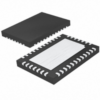
LTC4245CUHF#PBF Linear Technology, LTC4245CUHF#PBF Datasheet - Page 28

LTC4245CUHF#PBF
Manufacturer Part Number
LTC4245CUHF#PBF
Description
IC CNTRLR HOT SWAP 38-QFN
Manufacturer
Linear Technology
Type
Hot-Swap Controllerr
Datasheet
1.LTC4245CUHFPBF.pdf
(36 pages)
Specifications of LTC4245CUHF#PBF
Applications
CompactPCI™
Internal Switch(s)
No
Voltage - Supply
3.3V, 5V, 12V
Operating Temperature
0°C ~ 70°C
Mounting Type
Surface Mount
Package / Case
38-WFQFN, Exposed Pad
Family Name
LTC4245
Package Type
QFN EP
Operating Supply Voltage (min)
2.25/4.25/10.2/-10.2V
Operating Supply Voltage (max)
0/10/20/-20V
Operating Temperature (min)
0C
Operating Temperature (max)
70C
Operating Temperature Classification
Commercial
Product Depth (mm)
5mm
Product Length (mm)
7mm
Mounting
Surface Mount
Pin Count
38
Lead Free Status / RoHS Status
Lead free / RoHS Compliant
Available stocks
Company
Part Number
Manufacturer
Quantity
Price
APPLICATIO S I FOR ATIO
LTC4245
PCB Layout Considerations
For proper operation of the LTC4245’s circuit breaker,
Kelvin connection to the sense resistors is strongly
recommended. The PCB layout should be balanced and
symmetrical to minimize wiring errors. In addition, the
PCB layout for the sense resistors and the power MOSFETs
should include good thermal management techniques for
optimal device power dissipation. A recommended PCB
layout for the 5V sense resistor and the power MOSFET
around the LTC4245 is illustrated in Figure 18. In Hot Swap
applications where load currents can be 10A, narrow PCB
tracks exhibit more resistance than wider tracks and operate
28
at more elevated temperatures. Since the sheet resistance
of 1 ounce copper foil is approximately 0.5mΩ/o, track
resistances and voltage drops add up quickly in high current
applications. Thus, to keep PCB track resistance, voltage
U
5V
IN
TRACK WIDTH W:
0.03" PER AMPERE
ON 1 OZ Cu FOIL
CURRENT FLOW
U
Figure 18. Recommended Layout for R2, Q2, R6, Z2, C1, Z1, R10 and C2
TO LOAD
W
GND
*ADDITIONAL DETAILS OMITTED FOR CLARITY
DRAWING IS NOT TO SCALE!
Z2
W
CURRENT FLOW
TO SOURCE
RESISTOR
R2 SENSE
W
U
Z1
D
D
D
D
LTC4245G*
R6
R10
C2
SO-8
Q2
drop and temperature rise to a minimum, the suggested
trace width in these applications for 1oz copper foil is
0.03” for each ampere of DC current.
In the majority of applications, it will be necessary to use
plated-through vias to make circuit connections from
component layers to power and ground layers internal
to the PCB. For 1oz copper foil plating, a general rule is
1A of DC current per via, making sure the via is properly
dimensioned so that solder completely fi lls any void. For
other plating thicknesses, check with your PCB fabrica-
tion facility.
It is also important to put C1, the bypass capacitor for the
INTV
The surge suppressors, Z1 and Z2, are placed between the
supply inputs and ground using wide traces.
G
S
S
S
CC
CURRENT FLOW
pin as close as possible between INTV
C1
TO LOAD
W
VIA TO
GND PLANE
VIA TO
GND PLANE
5V
OUT
4245 F18
GND
CC
and GND.
4245fa


