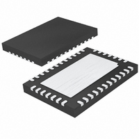
LTC4245CUHF#PBF Linear Technology, LTC4245CUHF#PBF Datasheet - Page 25

LTC4245CUHF#PBF
Manufacturer Part Number
LTC4245CUHF#PBF
Description
IC CNTRLR HOT SWAP 38-QFN
Manufacturer
Linear Technology
Type
Hot-Swap Controllerr
Datasheet
1.LTC4245CUHFPBF.pdf
(36 pages)
Specifications of LTC4245CUHF#PBF
Applications
CompactPCI™
Internal Switch(s)
No
Voltage - Supply
3.3V, 5V, 12V
Operating Temperature
0°C ~ 70°C
Mounting Type
Surface Mount
Package / Case
38-WFQFN, Exposed Pad
Family Name
LTC4245
Package Type
QFN EP
Operating Supply Voltage (min)
2.25/4.25/10.2/-10.2V
Operating Supply Voltage (max)
0/10/20/-20V
Operating Temperature (min)
0C
Operating Temperature (max)
70C
Operating Temperature Classification
Commercial
Product Depth (mm)
5mm
Product Length (mm)
7mm
Mounting
Surface Mount
Pin Count
38
Lead Free Status / RoHS Status
Lead free / RoHS Compliant
Available stocks
Company
Part Number
Manufacturer
Quantity
Price
APPLICATIO S I FOR ATIO
toggles, bit F7 is set to indicate a change of state. If the
GPIO1 alert bit B7 is enabled, this feature can be used to
alert the host system to a change in state of the board’s
ejector handles.
Compensating the Active Current Loop
The four active current limit circuits of the LTC4245 are
compensated internally and therefore do not require any
RC network on the gate pins. The internal compensation
should work for most pass transistors. If the gate capaci-
tance is very small then the best method to compensate
the loop is to add a 1nF to 5nF capacitor between the gate
and source of the external MOSFET.
Supply Collapse During Transients
The LTC4245 is designed to ride through supply transients
caused by load steps. If there is a shorted load and the
parasitic inductance back to the supply is signifi cant, there
is a chance that the supply could collapse before the active
current limit circuit brings down the gate of the external
MOSFET. In this case the undervoltage lockout circuit,
which has a 3.5μs (5.5μs for V
the pass transistors.
Input Overvoltage Transient Protection
Hot-plugging a board into a backplane generates inrush
currents from the backplane power supplies due to the
charging of the plug-in board capacitance. To reduce this
transient current to a safe level, the CPCI Hot Swap speci-
fi cation restricts the amount of unswitched capacitance
used on the input side of the plug-in board. Each medium
or long power pin connected to the CPCI female connector
on the plug-in board is required to have a 10nF ceramic
bypass capacitor to ground. Bulk capacitors are allowed
on the switched output side of the LTC4245. Some bulk
capacitance is allowed on the Early Power planes, but only
because a current limiting resistor is assumed to decouple
the connector pin from the bulk capacitance (e.g., see
100Ω to Bus Switch V
Disallowing bulk capacitors on the input power pins tends
to create a resonant circuit formed by the inductance of
the backplane power supply trace and the parasitic capaci-
tance of the plug-in board (mainly due to the large power
U
DD
in Figure 10).
U
EEIN
W
) fi lter time, turns off
U
MOSFET). Upon board insertion, the ringing of this circuit
can exhibit a peak overshoot of 2.5 times the steady-state
voltage (>30V for 12V
There are two methods for abating the effects of these
high voltage transients: using voltage limiters to clip the
transient to a safe level and snubber networks. Snubber
networks are series RC networks whose time constants are
experimentally determined based on the board’s parasitic
resonance circuits. As a starting point, the capacitors in
these networks are chosen to be 10× to 100× the power
MOSFET’s C
determined experimentally that ranges from 1Ω to 50Ω,
depending on the parasitic resonance circuit. Note that
in all LTC4245 circuit schematics, both transient voltage
limiters and snubber networks have been added to the
12V
Snubber networks are not necessary on the 3V
5V
10V. Transient voltage limiters, however, are recommended
as these devices provide large-scale transient protection
for the LTC4245 in the event of abrupt changes in supply
current. All protection networks should be mounted very
close to the LTC4245’s supply pins using short lead lengths
to minimize the trace resistance and inductance. A rec-
ommended layout of the 5V and 12V transient protection
devices around the LTC4245 is shown in Figure 18.
Design Example
As a design example, consider a Hot Swap application
with the following power supply requirements:
Table 1. Example Power Supply Requirements
1. Select the appropriate values of R
Calculating the value of R
and the lower limit for the circuit breaker threshold volt-
age, ΔV
sense resistors, then the following values of resistances
should suffi ce:
IN
VOLTAGE
SUPPLY
IN
supply lines since their absolute maximum ratings are
–12V
3.3V
12V
5V
and V
SNS(CB)(MIN)
EEIN
OSS
under bias. The series resistor is a value
supply rails and should always be used.
MAXIMUM
CURRENT
600mA
300mA
LOAD
. If a 1% tolerance is assumed for the
5A
7A
IN
).
SENSE
INRUSH dI/dt
MAXIMUM
150mA/ms
150mA/ms
1.5A/ms
1.5A/ms
is based on I
SENSE
LTC4245
for the supplies.
CAPACITANCE
2200μF
2200μF
LOAD(MAX)
100μF
100μF
LOAD
IN
25
or the
4245fa


