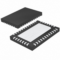
LTC4245CUHF#PBF Linear Technology, LTC4245CUHF#PBF Datasheet - Page 6

LTC4245CUHF#PBF
Manufacturer Part Number
LTC4245CUHF#PBF
Description
IC CNTRLR HOT SWAP 38-QFN
Manufacturer
Linear Technology
Type
Hot-Swap Controllerr
Datasheet
1.LTC4245CUHFPBF.pdf
(36 pages)
Specifications of LTC4245CUHF#PBF
Applications
CompactPCI™
Internal Switch(s)
No
Voltage - Supply
3.3V, 5V, 12V
Operating Temperature
0°C ~ 70°C
Mounting Type
Surface Mount
Package / Case
38-WFQFN, Exposed Pad
Family Name
LTC4245
Package Type
QFN EP
Operating Supply Voltage (min)
2.25/4.25/10.2/-10.2V
Operating Supply Voltage (max)
0/10/20/-20V
Operating Temperature (min)
0C
Operating Temperature (max)
70C
Operating Temperature Classification
Commercial
Product Depth (mm)
5mm
Product Length (mm)
7mm
Mounting
Surface Mount
Pin Count
38
Lead Free Status / RoHS Status
Lead free / RoHS Compliant
Available stocks
Company
Part Number
Manufacturer
Quantity
Price
LTC4245
SYMBOL
t
t
t
t
C
t
Note 1: Stresses beyond those listed under Absolute Maximum Ratings
may cause permanent damage to the device. Exposure to any Absolute
Maximum Rating condition for extended periods may affect device
reliability and lifetime.
Note 2: All currents into device pins are positive; all currents out of device
pins are negative. All voltages are referenced to GND unless otherwise
specifi ed.
Note 3: The 5V
lower of 12V
Note 4: An internal clamp limits the GATE pins to a minimum of 5V above
V
may damage the device.
TI I G DIAGRA
ELECTRICAL CHARACTERISTICS
range, otherwise specifi cations are at T
6
SU, DAT(MIN)
HD, DATI(MIN)
HD, DATO(MIN)
SP(MAX)
of
X
OUT
W U
(V
EEIN
for V
IN
GATE
+ 0.3V and 14V.
EEGATE
t
SDA
HD, STA
SCL
and 3V
PARAMETER
Minimum Data Set-Up Time Input
Minimum Data Hold Time Input
Minimum Data Hold Time Output
Maximum Suppressed Spike Pulse Width
SCL, SDA Input Capacitance
Data Output Fall Time
). Driving this pin to voltages beyond the clamp
CONDITION
START
GATE
pins should not be driven beyond the
W
A
t
SU, DAT
= 25°C. V
t
of
12VIN
t
t
HD, DATO,
HD, DATI
= 12V, V
CONDITIONS
(Note 9)
The
5VIN
REPEATED START
●
= 5V, V
CONDITION
denotes the specifi cations which apply over the full operating temperature
Note 5: The device pulls up the V
Note 6: UHF package specifi cation limits are identical to G package limits
and guaranteed by design and by correlation to wafer test measurements.
Note 7: Guaranteed by design and not subject to test.
Note 8: Integral Nonlinearity is defi ned as the deviation of a code from a
precise analog input voltage. Maximum specifi cations are limited by the
LSB step size and the single shot measurement. Typical specifi cations are
measured from 1/4, 1/2, 3/4 areas of the quantization band.
Note 9: C
t
SU, STA
3VIN
= 3.3V, V
t
HD, STA
b
= total capacitance of one bus line in pF.
t
SP
t
SP
VEEIN
t
SU, STO
= –12V, unless otherwise noted.
CONDITION
20 + 0.1C
STOP
EEOUT
MIN
300
50
pin to 0.6V when pin is in open state.
t
BUF
b
CONDITION
–100
TYP
500
110
START
0
5
4245 TDO1
MAX
100
900
250
250
10
0
UNITS
4245fa
ns
ns
ns
ns
pF
ns


