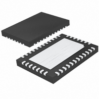
LTC4245CUHF#PBF Linear Technology, LTC4245CUHF#PBF Datasheet - Page 17

LTC4245CUHF#PBF
Manufacturer Part Number
LTC4245CUHF#PBF
Description
IC CNTRLR HOT SWAP 38-QFN
Manufacturer
Linear Technology
Type
Hot-Swap Controllerr
Datasheet
1.LTC4245CUHFPBF.pdf
(36 pages)
Specifications of LTC4245CUHF#PBF
Applications
CompactPCI™
Internal Switch(s)
No
Voltage - Supply
3.3V, 5V, 12V
Operating Temperature
0°C ~ 70°C
Mounting Type
Surface Mount
Package / Case
38-WFQFN, Exposed Pad
Family Name
LTC4245
Package Type
QFN EP
Operating Supply Voltage (min)
2.25/4.25/10.2/-10.2V
Operating Supply Voltage (max)
0/10/20/-20V
Operating Temperature (min)
0C
Operating Temperature (max)
70C
Operating Temperature Classification
Commercial
Product Depth (mm)
5mm
Product Length (mm)
7mm
Mounting
Surface Mount
Pin Count
38
Lead Free Status / RoHS Status
Lead free / RoHS Compliant
Available stocks
Company
Part Number
Manufacturer
Quantity
Price
APPLICATIO S I FOR ATIO
Turn-Off
The switches can be turned off by a variety of condi-
tions.
Normally the 12V, 5V and 3.3V switches are turned off
with a 1.3mA current pulling down the gate to ground.
V
supply outputs are also discharged to ground through
internal switches. When any MOSFET is shut off, the
HEALTHY# signal pulls high and LOCAL_PCI_RST# will
be asserted low. Figure 4 shows all supplies being turned
off by BD_SEL# going high.
ON Register and Sequencing
The LTC4245 features an ON register (Table 10) consisting
of four On control bits (D0 to D3) and four On status bits
(D4 to D7). D0 to D3 provide independent on/off control
for each supply through the I
EEGATE
1. ON pin going low or BD_SEL# going high turns off all
2. Individual switches can be turned off by resetting
3. A variety of fault conditions will turn off all switches
4. Writing a logic one into the undervoltage, overcurrent
3V
switches.
the particular FET On control bit (D0 to D3) through
the serial bus.
together. These include supply undervoltage,
overcurrent circuit breaker and PGI faults.
or PGI fault bits will turn off all switches, if the
corresponding autoretry is not enabled.
OUT
is pulled through a resistive switch to V
LOCAL_PCI_RST#
, V
EEOUT
12V
Figure 4. Normal Turn-Off Waveform
OUT
HEALTHY#
BD_SEL#
, 10V/DIV
, 5V
5V/DIV
5V/DIV
5V/DIV
OUT
U
U
2
C bus. Bits D4 to D7 report
TIME 100ms/DIV
W
U
4245 F04
EEIN
. All
bits get set one after another, leading to a 12V, 5V, 3.3V,
–12V start-up sequence. Figure 5 illustrates this. If C6 is set
and any of the start-up conditions goes bad, all switches
turn-off, and all On control bits except D0 are reset. This
ensures that the part goes through a sequenced turn-on
during auto-retry. D1 to D3 are also reset when BD_SEL#
goes low with C6 set.
the on status of each supply. Even though a supply may
be commanded to turn-on by setting its On control bit,
it may remain off (On status bit low) because the condi-
tions to turn on, as listed in the Turn-On section, may not
be present.
The sequence control bit, C6, determines whether the four
supply MOSFETs turn-on together or in a fi xed sequence.
The default state is no sequencing. In this case taking
the ON pin high sets all the four On control bits. If the
start-up conditions are satisfi ed, all switches will turn on
under the control of a single TIMER and SS cycle. Due to
different input voltage offsets in the current limit amplifi er
of each supply, the gate turn-on of all MOSFETs will not
occur at the same moment but will happen in random
order depending on amplifi er offset and soft-start ramp
rate. The gate turn-ons will be truly simultaneous only if
SS pin is left open.
If bit C6 is set, then the ON pin going high sets only the
12V On control bit, D0. The 12V back-end supply ramps
up. The end of the TIMER and SS cycle sets the 5V On
control bit, D1, starting the ramp of the 5V supply output.
The end of the 5V timing cycle sets bit D2 and the end of
the 3.3V ramp sets bit D3. In this way, the four On control
3V
OUT
LOCAL_PCI_RST#
, V
EEOUT
12V
Figure 5. Sequential Turn-On Waveform
OUT
HEALTHY#
, 10V/DIV
BD_SEL#
2.5V/DIV
2.5V/DIV
, 5V
5V/DIV
5V/DIV
5V/DIV
TIMER
OUT
SS
TIME 50ms/DIV
LTC4245
4245 F05
17
4245fa


