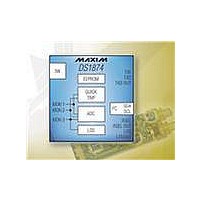
DS1874T+ Maxim Integrated Products, DS1874T+ Datasheet - Page 16

DS1874T+
Manufacturer Part Number
DS1874T+
Description
IC CTLR SFP+ ANLG LDD 28-TQFN
Manufacturer
Maxim Integrated Products
Type
Laser Diode Controllerr
Datasheet
1.DS1874TTR.pdf
(88 pages)
Specifications of DS1874T+
Number Of Channels
1
Voltage - Supply
2.85 V ~ 3.9 V
Current - Supply
2.5mA
Operating Temperature
-40°C ~ 95°C
Package / Case
28-WFQFN Exposed Pad
Mounting Type
Surface Mount
Number Of Outputs
5
Duty Cycle (max)
50 %
Output Voltage
0 V to 3.9 V
Mounting Style
SMD/SMT
Switching Frequency
0 KHz to 400 KHz
Operating Supply Voltage
2.85 V to 3.9 V
Supply Current
2.5 mA to 10 mA
Maximum Operating Temperature
+ 95 C
Fall Time
300 ns
Minimum Operating Temperature
- 40 C
Rise Time
300 ns
Synchronous Pin
Yes
Lead Free Status / RoHS Status
Lead free / RoHS Compliant
Other names
90-1874T+000
SFP+ Controller with Digital LDD Interface
ignored until the end of the 3-wire communication that
updates the MAX3798/MAX3799’s BIAS DAC, plus an
additional 16 sample periods (t
Monitoring functions on the DS1874 include five quick-trip
comparators and six ADC channels. This monitoring
combined with the alarm enables (Table 01h/05h) deter-
mines when/if the DS1874 turns off the MAX3798/
MAX3799 DACs and triggers the TXF and TXDOUT out-
puts. All the monitoring levels and interrupt masks are
user programmable.
Five quick-trip monitors are provided to detect potential
laser safety issues and LOS status. These monitor the
following:
1) High Bias Current (HBATH)
2) Low Transmit Power (LTXP)
3) High Transmit Power (HTXP)
4) Max Output Current (IBIASMAX)
5) Loss-of-Signal (LOS LO)
The high-transmit and low-transmit power quick-trip reg-
isters (HTXP and LTXP) set the thresholds used to com-
pare against the MON2 voltage to determine if the
transmit power is within specification. The HBATH quick
trip compares the MON1 input (generally from the
MAX3798/MAX3799 bias monitor output) against its
threshold setting to determine if the present bias current
is above specification. The BIAS MAX quick trip deter-
mines if the BIAS register is above specification. The
BIAS register is not allowed to exceed the value set in
the IBIASMAX register. When the DS1874 detects that
the bias is at the limit it sets the BIAS MAX status bit
and holds the BIAS register setting at the IBIASMAX
level. The bias and power quick trips are routed to the
TXF through interrupt masks to allow combinations of
these alarms to be used to trigger these outputs. The
user can program up to eight different temperature-
indexed threshold levels for MON1 (Table 02h,
Registers D0h–D7h). The LOS LO quick trip compares
the MON3 input against its threshold setting to deter-
mine if the present received power is below the specifi-
cation. The LOS LO quick trip can be used to set the
LOSOUT pin. These alarms can be latched using Table
02h, Register 8Ah.
The ADC monitors six channels that measure tempera-
ture (internal temp sensor), V
using an analog multiplexer to measure them round
16
______________________________________________________________________________________
Five Quick-Trip Monitors and Alarms
Monitors and Fault Detection
Six ADC Monitors and Alarms
REP
CC
, and MON1–MON4
).
Monitors
robin with a single ADC (see the ADC Timing section).
The five voltage channels have a customer-programma-
ble full-scale range and all channels have a customer-
programmable offset value that is factory programmed to
default value (see Table 3). Additionally, MON1–MON4
can right-shift results by up to 7 bits before the results
are compared to alarm thresholds or read over the I
bus. This allows customers with specified ADC ranges to
calibrate the ADC full scale to a factor of 1/2
specified range to measure small signals. The DS1874
can then right-shift the results by n bits to maintain the bit
weight of their specification (see the Right-Shifting ADC
Result and Enhanced RSSI Monitoring (Dual-Range
Functionality) sections).
The ADC results (after right-shifting, if used) are com-
pared to the alarm and warning thresholds after each
conversion, and the corresponding alarms are set,
which can be used to trigger the TXF output. These
ADC thresholds are user programmable, as are the
masking registers that can be used to prevent the
alarms from triggering the TXF output.
There are six analog channels that are digitized in a
round-robin fashion in the order shown in Figure 5. The
total time required to convert all six channels is t
the Analog Voltage Monitoring Characteristics for details).
If the weighting of the ADC digital reading must con-
form to a predetermined full-scale (PFS) value defined
by a standard’s specification (e.g., SFF-8472), then
right-shifting can be used to adjust the PFS analog
measurement range while maintaining the weighting of
the ADC results. The DS1874’s range is wide enough to
cover all requirements; when the maximum input value
is ≤ 1/2 of the FS value, right-shifting can be used to
obtain greater accuracy. For instance, the maximum
voltage might be 1/8 the specified PFS value, so only
1/8 the converter’s range is effective over this range.
An alternative is to calibrate the ADC’s full-scale range
to 1/8 the readable PFS value and use a right-shift
value of 3. With this implementation, the resolution of
Table 3. ADC Default Monitor Full-Scale
Ranges
Temperature (°C)
V
MON1–MON4 (V)
CC
(V)
SIGNAL
SIGNAL
127.996
6.5528
2.4997
+FS
Right-Shifting ADC Result
7FFF
FFF8
FFF8
+FS
hex
SIGNAL
-128
-FS
0
0
ADC Timing
n
RR
of their
8000
0000
0000
hex
-FS
(see
2
C


