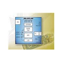
DS1874T+ Maxim Integrated Products, DS1874T+ Datasheet - Page 61

DS1874T+
Manufacturer Part Number
DS1874T+
Description
IC CTLR SFP+ ANLG LDD 28-TQFN
Manufacturer
Maxim Integrated Products
Type
Laser Diode Controllerr
Datasheet
1.DS1874TTR.pdf
(88 pages)
Specifications of DS1874T+
Number Of Channels
1
Voltage - Supply
2.85 V ~ 3.9 V
Current - Supply
2.5mA
Operating Temperature
-40°C ~ 95°C
Package / Case
28-WFQFN Exposed Pad
Mounting Type
Surface Mount
Number Of Outputs
5
Duty Cycle (max)
50 %
Output Voltage
0 V to 3.9 V
Mounting Style
SMD/SMT
Switching Frequency
0 KHz to 400 KHz
Operating Supply Voltage
2.85 V to 3.9 V
Supply Current
2.5 mA to 10 mA
Maximum Operating Temperature
+ 95 C
Fall Time
300 ns
Minimum Operating Temperature
- 40 C
Rise Time
300 ns
Synchronous Pin
Yes
Lead Free Status / RoHS Status
Lead free / RoHS Compliant
Other names
90-1874T+000
Table 02h, Register 8Bh: CNFGC
Table 02h, Register 8Ch: DEVICE ADDRESS
8Bh
8Ch
FACTORY DEFAULT
READ ACCESS
WRITE ACCESS
MEMORY TYPE
FACTORY DEFAULT
READ ACCESS
WRITE ACCESS
MEMORY TYPE
This value becomes the I
set. If A0h is programmed to this register, the auxiliary memory is disabled.
RESERVED
SFP+ Controller with Digital LDD Interface
BITS 7:6
BITS 1:0
BIT 7
BIT 5
BIT 4
BIT 3
BIT 2
BIT 7
2
______________________________________________________________________________________
7
RESERVED
TXDM34: Enables TXD to reset alarms and warnings associated to MON3 and MON4 during a TXD
event.
0 = TXD event has no effect on the MON3 and MON4 alarms, warnings, and quick trips.
1 = MON3 and MON4 alarms, warnings, and quick trips are reset during a TXD event.
TXDFG: See Figure 12.
0 = FETG, an internal signal, has no effect on TXDOUT.
1 = FETG is enabled and ORed with other possible signals to create TXDOUT.
TXDFLT: See Figure 12.
0 = TXF pin has no effect on TXDOUT.
1 = TXF pin is enabled and ORed with other possible signals to create TXDOUT.
TXDIO: See Figure 12.
0 = (Default) TXD input signal is enabled and ORed with other possible signals to create TXDOUT.
1 = TXD input signal has no effect on TXDOUT.
RSSI_FC and RSSI_FF: RSSI Force Coarse and RSSI Force Fine. Control bits for RSSI mode of
operation on the MON3 conversion.
00b = Normal RSSI mode of operation (default).
01b = The fine settings of scale and offset are used for MON3 conversions.
10b = The coarse settings of scale and offset are used for MON3 conversions.
11b = Normal RSSI mode of operation.
RESERVED
2
6
2
C slave address for the main memory when the ASEL (Table 02h, Register 89h) bit is
00h
PW2 or (PW1 and RWTBL246) or (PW1 and RTBL246)
PW2 or (PW1 and RWTBL246)
Nonvolatile (SEE)
00h
PW2 or (PW1 and RWTBL246) or (PW1 and RTBL246)
PW2 or (PW1 and RWTBL246)
Nonvolatile (SEE)
TXDM34
2
5
TXDFG
2
4
TXDFLT
2
3
TXDIO
2
2
RSSI_FC
2
1
RSSI_FF
BIT 0
BIT 0
2
0
61


