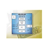
DS1874T+ Maxim Integrated Products, DS1874T+ Datasheet - Page 51

DS1874T+
Manufacturer Part Number
DS1874T+
Description
IC CTLR SFP+ ANLG LDD 28-TQFN
Manufacturer
Maxim Integrated Products
Type
Laser Diode Controllerr
Datasheet
1.DS1874TTR.pdf
(88 pages)
Specifications of DS1874T+
Number Of Channels
1
Voltage - Supply
2.85 V ~ 3.9 V
Current - Supply
2.5mA
Operating Temperature
-40°C ~ 95°C
Package / Case
28-WFQFN Exposed Pad
Mounting Type
Surface Mount
Number Of Outputs
5
Duty Cycle (max)
50 %
Output Voltage
0 V to 3.9 V
Mounting Style
SMD/SMT
Switching Frequency
0 KHz to 400 KHz
Operating Supply Voltage
2.85 V to 3.9 V
Supply Current
2.5 mA to 10 mA
Maximum Operating Temperature
+ 95 C
Fall Time
300 ns
Minimum Operating Temperature
- 40 C
Rise Time
300 ns
Synchronous Pin
Yes
Lead Free Status / RoHS Status
Lead free / RoHS Compliant
Other names
90-1874T+000
Table 01h, Register FAh: ALARM EN
FAh
POWER-ON VALUE
READ ACCESS
WRITE ACCESS
MEMORY TYPE
Layout is identical to ALARM
Figure 12) logic. The MASK bit (Table 02h, Register 89h) determines whether this memory exists in Table 01h or
05h.
RESERVED
SFP+ Controller with Digital LDD Interface
BITS 7:4
BIT 7
BIT 3
BIT 2
BIT 1
BIT 0
______________________________________________________________________________________
RESERVED
HBAL:
0 = Disables interrupt from HBAL alarm.
1 = Enables interrupt from HBAL alarm.
RESERVED
TXP HI:
0 = Disables interrupt from TXP HI alarm.
1 = Enables interrupt from TXP HI alarm.
TXP LO:
0 = Disables interrupt from TXP LO alarm.
1 = Enables interrupt from TXP LO alarm.
RESERVED
00h
PW2 or (PW1 and RWTBL1C) or (PW1 and RTBL1C)
PW2 or (PW1 and RWTBL1C)
Nonvolatile (SEE)
1
1
RESERVED
in Lower Memory, Register 72h. Enables alarms to create internal signal FETG (see
RESERVED
HBAL
RESERVED
TXP HI
TXP LO
BIT 0
51


