C8051F350DK Silicon Laboratories Inc, C8051F350DK Datasheet - Page 122
C8051F350DK
Manufacturer Part Number
C8051F350DK
Description
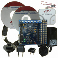
DEV KIT FOR F350/351/352/353
Manufacturer
Silicon Laboratories Inc
Type
MCUr
Specifications of C8051F350DK
Contents
Evaluation Board, Power Supply, USB Cables, Adapter and Documentation
Processor To Be Evaluated
C8051F35x
Interface Type
USB
Silicon Manufacturer
Silicon Labs
Core Architecture
8051
Silicon Core Number
C8051F350
Silicon Family Name
C8051F35x
Lead Free Status / RoHS Status
Contains lead / RoHS non-compliant
For Use With/related Products
C8051F350, 351, 352, 353
Lead Free Status / Rohs Status
Lead free / RoHS Compliant
Other names
336-1083
Available stocks
Company
Part Number
Manufacturer
Quantity
Price
Company:

Part Number:
C8051F350DK
Manufacturer:
SiliconL
Quantity:
8


C8051F350/1/2/3
15.1.3. Flash Write Procedure
Bytes in Flash memory can be written one byte at a time, or in groups of two. The FLBWE bit in register
PFE0CN (SFR Definition 13.1) controls whether a single byte or a block of two bytes is written to Flash
during a write operation. When FLBWE is cleared to ‘0’, the Flash will be written one byte at a time. When
FLBWE is set to ‘1’, the Flash will be written in two-byte blocks. Block writes are performed in the same
amount of time as single-byte writes, which can save time when storing large amounts of data to Flash
memory.
During a single-byte write to Flash, bytes are written individually, and a Flash write will be performed after
each MOVX write instruction. The recommended procedure for writing Flash in single bytes is:
Steps 5–7 must be repeated for each byte to be written.
For block Flash writes, the Flash write procedure is only performed after the last byte of each block is writ-
ten with the MOVX write instruction. A Flash write block is two bytes long, from even addresses to odd
addresses. Writes must be performed sequentially (i.e. addresses ending in 0b and 1b must be written in
order). The Flash write will be performed following the MOVX write that targets the address ending in 1b. If
a byte in the block does not need to be updated in Flash, it should be written to 0xFF. The recommended
procedure for writing Flash in blocks is:
Steps 5–10 must be repeated for each block to be written.
122
Step 1. Disable interrupts.
Step 2. Clear the FLBWE bit (register PFE0CN) to select single-byte write mode.
Step 3. Set the PSWE bit (register PSCTL).
Step 4. Clear the PSEE bit (register PSCTL).
Step 5. Write the first key code to FLKEY: 0xA5.
Step 6. Write the second key code to FLKEY: 0xF1.
Step 7. Using the MOVX instruction, write a single data byte to the desired location within the 512-
Step 8. Clear the PSWE bit.
Step 9. Re-enable interrupts.
Step 1. Disable interrupts.
Step 2. Set the FLBWE bit (resgister PFE0CN) to select block write mode.
Step 3. Set the PSWE bit (register PSCTL).
Step 4. Clear the PSEE bit (register PSCTL).
Step 5. Write the first key code to FLKEY: 0xA5.
Step 6. Write the second key code to FLKEY: 0xF1.
Step 7. Using the MOVX instruction, write the first data byte to the even block location (ending in
Step 8. Write the first key code to FLKEY: 0xA5.
Step 9. Write the second key code to FLKEY: 0xF1.
Step 10. Using the MOVX instruction, write the second data byte to the odd block location (ending
Step 11. Clear the PSWE bit.
Step 12. Re-enable interrupts.
0b).
in 1b).
byte sector.
Rev. 1.1
Related parts for C8051F350DK
Image
Part Number
Description
Manufacturer
Datasheet
Request
R

Part Number:
Description:
SMD/C°/SINGLE-ENDED OUTPUT SILICON OSCILLATOR
Manufacturer:
Silicon Laboratories Inc
Part Number:
Description:
Manufacturer:
Silicon Laboratories Inc
Datasheet:
Part Number:
Description:
N/A N/A/SI4010 AES KEYFOB DEMO WITH LCD RX
Manufacturer:
Silicon Laboratories Inc
Datasheet:
Part Number:
Description:
N/A N/A/SI4010 SIMPLIFIED KEY FOB DEMO WITH LED RX
Manufacturer:
Silicon Laboratories Inc
Datasheet:
Part Number:
Description:
N/A/-40 TO 85 OC/EZLINK MODULE; F930/4432 HIGH BAND (REV E/B1)
Manufacturer:
Silicon Laboratories Inc
Part Number:
Description:
EZLink Module; F930/4432 Low Band (rev e/B1)
Manufacturer:
Silicon Laboratories Inc
Part Number:
Description:
I°/4460 10 DBM RADIO TEST CARD 434 MHZ
Manufacturer:
Silicon Laboratories Inc
Part Number:
Description:
I°/4461 14 DBM RADIO TEST CARD 868 MHZ
Manufacturer:
Silicon Laboratories Inc
Part Number:
Description:
I°/4463 20 DBM RFSWITCH RADIO TEST CARD 460 MHZ
Manufacturer:
Silicon Laboratories Inc
Part Number:
Description:
I°/4463 20 DBM RADIO TEST CARD 868 MHZ
Manufacturer:
Silicon Laboratories Inc
Part Number:
Description:
I°/4463 27 DBM RADIO TEST CARD 868 MHZ
Manufacturer:
Silicon Laboratories Inc
Part Number:
Description:
I°/4463 SKYWORKS 30 DBM RADIO TEST CARD 915 MHZ
Manufacturer:
Silicon Laboratories Inc
Part Number:
Description:
N/A N/A/-40 TO 85 OC/4463 RFMD 30 DBM RADIO TEST CARD 915 MHZ
Manufacturer:
Silicon Laboratories Inc
Part Number:
Description:
I°/4463 20 DBM RADIO TEST CARD 169 MHZ
Manufacturer:
Silicon Laboratories Inc