C8051F350DK Silicon Laboratories Inc, C8051F350DK Datasheet - Page 127
C8051F350DK
Manufacturer Part Number
C8051F350DK
Description
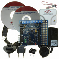
DEV KIT FOR F350/351/352/353
Manufacturer
Silicon Laboratories Inc
Type
MCUr
Specifications of C8051F350DK
Contents
Evaluation Board, Power Supply, USB Cables, Adapter and Documentation
Processor To Be Evaluated
C8051F35x
Interface Type
USB
Silicon Manufacturer
Silicon Labs
Core Architecture
8051
Silicon Core Number
C8051F350
Silicon Family Name
C8051F35x
Lead Free Status / RoHS Status
Contains lead / RoHS non-compliant
For Use With/related Products
C8051F350, 351, 352, 353
Lead Free Status / Rohs Status
Lead free / RoHS Compliant
Other names
336-1083
Available stocks
Company
Part Number
Manufacturer
Quantity
Price
Company:

Part Number:
C8051F350DK
Manufacturer:
SiliconL
Quantity:
8


16. External RAM
The C8051F350/1/2/3 devices include 512 bytes of RAM mapped into the external data memory space. All
of these address locations may be accessed using the external move instruction (MOVX) and the data
pointer (DPTR), or using MOVX indirect addressing mode. If the MOVX instruction is used with an 8-bit
address operand (such as @R1), then the high byte of the 16-bit address is provided by the External Mem-
ory Interface Control Register (EMI0CN as shown in SFR Definition 16.1). Note: the MOVX instruction is
also used for writes to the Flash memory. See Section “15. Flash Memory’ on page 121 for details. The
MOVX instruction accesses XRAM by default.
For a 16-bit MOVX operation (@DPTR), the upper 7-bits of the 16-bit external data memory address word
are "don't cares". As a result, the 512-byte RAM is mapped modulo style over the entire 64 k external data
memory address range. For example, the XRAM byte at address 0x0000 is shadowed at addresses
0x0200, 0x0400, 0x0600, 0x0800, etc. This is a useful feature when performing a linear memory fill, as the
address pointer doesn't have to be reset when reaching the RAM block boundary.
Bits 7–1: UNUSED. Read = 0000000b. Write = don’t care.
Bit 0:
R/W
Bit7
—
SFR Definition 16.1. EMI0CN: External Memory Interface Control
PGSEL: XRAM Page Select.
The EMI0CN register provides the high byte of the 16-bit external data memory address
when using an 8-bit MOVX command, effectively selecting a 256-byte page of RAM. Since
the upper (unused) bits of the register are always zero, the PGSEL determines which page
of XRAM is accessed.
For Example: If EMI0CN = 0x01, addresses 0x0100 through 0x01FF will be accessed.
R/W
Bit6
—
R/W
Bit5
—
R/W
Bit4
—
Rev. 1.1
R/W
Bit3
—
R/W
Bit2
—
C8051F350/1/2/3
R/W
Bit1
—
SFR Address:
PGSEL
R/W
Bit0
0xAA
00000000
Reset Value
127
Related parts for C8051F350DK
Image
Part Number
Description
Manufacturer
Datasheet
Request
R

Part Number:
Description:
SMD/C°/SINGLE-ENDED OUTPUT SILICON OSCILLATOR
Manufacturer:
Silicon Laboratories Inc
Part Number:
Description:
Manufacturer:
Silicon Laboratories Inc
Datasheet:
Part Number:
Description:
N/A N/A/SI4010 AES KEYFOB DEMO WITH LCD RX
Manufacturer:
Silicon Laboratories Inc
Datasheet:
Part Number:
Description:
N/A N/A/SI4010 SIMPLIFIED KEY FOB DEMO WITH LED RX
Manufacturer:
Silicon Laboratories Inc
Datasheet:
Part Number:
Description:
N/A/-40 TO 85 OC/EZLINK MODULE; F930/4432 HIGH BAND (REV E/B1)
Manufacturer:
Silicon Laboratories Inc
Part Number:
Description:
EZLink Module; F930/4432 Low Band (rev e/B1)
Manufacturer:
Silicon Laboratories Inc
Part Number:
Description:
I°/4460 10 DBM RADIO TEST CARD 434 MHZ
Manufacturer:
Silicon Laboratories Inc
Part Number:
Description:
I°/4461 14 DBM RADIO TEST CARD 868 MHZ
Manufacturer:
Silicon Laboratories Inc
Part Number:
Description:
I°/4463 20 DBM RFSWITCH RADIO TEST CARD 460 MHZ
Manufacturer:
Silicon Laboratories Inc
Part Number:
Description:
I°/4463 20 DBM RADIO TEST CARD 868 MHZ
Manufacturer:
Silicon Laboratories Inc
Part Number:
Description:
I°/4463 27 DBM RADIO TEST CARD 868 MHZ
Manufacturer:
Silicon Laboratories Inc
Part Number:
Description:
I°/4463 SKYWORKS 30 DBM RADIO TEST CARD 915 MHZ
Manufacturer:
Silicon Laboratories Inc
Part Number:
Description:
N/A N/A/-40 TO 85 OC/4463 RFMD 30 DBM RADIO TEST CARD 915 MHZ
Manufacturer:
Silicon Laboratories Inc
Part Number:
Description:
I°/4463 20 DBM RADIO TEST CARD 169 MHZ
Manufacturer:
Silicon Laboratories Inc