C8051F350DK Silicon Laboratories Inc, C8051F350DK Datasheet - Page 89
C8051F350DK
Manufacturer Part Number
C8051F350DK
Description
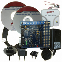
DEV KIT FOR F350/351/352/353
Manufacturer
Silicon Laboratories Inc
Type
MCUr
Specifications of C8051F350DK
Contents
Evaluation Board, Power Supply, USB Cables, Adapter and Documentation
Processor To Be Evaluated
C8051F35x
Interface Type
USB
Silicon Manufacturer
Silicon Labs
Core Architecture
8051
Silicon Core Number
C8051F350
Silicon Family Name
C8051F35x
Lead Free Status / RoHS Status
Contains lead / RoHS non-compliant
For Use With/related Products
C8051F350, 351, 352, 353
Lead Free Status / Rohs Status
Lead free / RoHS Compliant
Other names
336-1083
Available stocks
Company
Part Number
Manufacturer
Quantity
Price
Company:

Part Number:
C8051F350DK
Manufacturer:
SiliconL
Quantity:
8


10.1. Instruction Set
The instruction set of the CIP-51 System Controller is fully compatible with the standard MCS-51™ instruc-
tion set. Standard 8051 development tools can be used to develop software for the CIP-51. All CIP-51
instructions are the binary and functional equivalent of their MCS-51™ counterparts, including opcodes,
addressing modes and effect on PSW flags. However, instruction timing is different than that of the stan-
dard 8051.
10.1.1. Instruction and CPU Timing
In many 8051 implementations, a distinction is made between machine cycles and clock cycles, with
machine cycles varying from 2 to 12 clock cycles in length. However, the CIP-51 implementation is based
solely on clock cycle timing. All instruction timings are specified in terms of clock cycles.
Due to the pipelined architecture of the CIP-51, most instructions execute in the same number of clock
cycles as there are program bytes in the instruction. Conditional branch instructions take one less clock
cycle to complete when the branch is not taken as opposed to when the branch is taken. Table 10.1 is the
CIP-51 Instruction Set Summary, which includes the mnemonic, number of bytes, and number of clock
cycles for each instruction.
10.1.2. MOVX Instruction and Program Memory
The MOVX instruction is typically used to access data stored in XDATA memory space. In the CIP-51, the
MOVX instruction can also be used to write or erase on-chip program memory space implemented as re-
programmable Flash memory. The Flash access feature provides a mechanism for the CIP-51 to update
program code and use the program memory space for non-volatile data storage. Refer to Section
“15. Flash Memory’ on page 121 for further details.
ADD A, Rn
ADD A, direct
ADD A, @Ri
ADD A, #data
ADDC A, Rn
ADDC A, direct
ADDC A, @Ri
ADDC A, #data
SUBB A, Rn
SUBB A, direct
SUBB A, @Ri
SUBB A, #data
INC A
INC Rn
INC direct
INC @Ri
DEC A
DEC Rn
Mnemonic
Table 10.1. CIP-51 Instruction Set Summary
Add register to A
Add direct byte to A
Add indirect RAM to A
Add immediate to A
Add register to A with carry
Add direct byte to A with carry
Add indirect RAM to A with carry
Add immediate to A with carry
Subtract register from A with borrow
Subtract direct byte from A with borrow
Subtract indirect RAM from A with borrow
Subtract immediate from A with borrow
Increment A
Increment register
Increment direct byte
Increment indirect RAM
Decrement A
Decrement register
Arithmetic Operations
Description
Rev. 1.1
C8051F350/1/2/3
Bytes
1
2
1
2
1
2
1
2
1
2
1
2
1
1
2
1
1
1
Cycles
Clock
1
2
2
2
1
2
2
2
1
2
2
2
1
1
2
2
1
1
89
Related parts for C8051F350DK
Image
Part Number
Description
Manufacturer
Datasheet
Request
R

Part Number:
Description:
SMD/C°/SINGLE-ENDED OUTPUT SILICON OSCILLATOR
Manufacturer:
Silicon Laboratories Inc
Part Number:
Description:
Manufacturer:
Silicon Laboratories Inc
Datasheet:
Part Number:
Description:
N/A N/A/SI4010 AES KEYFOB DEMO WITH LCD RX
Manufacturer:
Silicon Laboratories Inc
Datasheet:
Part Number:
Description:
N/A N/A/SI4010 SIMPLIFIED KEY FOB DEMO WITH LED RX
Manufacturer:
Silicon Laboratories Inc
Datasheet:
Part Number:
Description:
N/A/-40 TO 85 OC/EZLINK MODULE; F930/4432 HIGH BAND (REV E/B1)
Manufacturer:
Silicon Laboratories Inc
Part Number:
Description:
EZLink Module; F930/4432 Low Band (rev e/B1)
Manufacturer:
Silicon Laboratories Inc
Part Number:
Description:
I°/4460 10 DBM RADIO TEST CARD 434 MHZ
Manufacturer:
Silicon Laboratories Inc
Part Number:
Description:
I°/4461 14 DBM RADIO TEST CARD 868 MHZ
Manufacturer:
Silicon Laboratories Inc
Part Number:
Description:
I°/4463 20 DBM RFSWITCH RADIO TEST CARD 460 MHZ
Manufacturer:
Silicon Laboratories Inc
Part Number:
Description:
I°/4463 20 DBM RADIO TEST CARD 868 MHZ
Manufacturer:
Silicon Laboratories Inc
Part Number:
Description:
I°/4463 27 DBM RADIO TEST CARD 868 MHZ
Manufacturer:
Silicon Laboratories Inc
Part Number:
Description:
I°/4463 SKYWORKS 30 DBM RADIO TEST CARD 915 MHZ
Manufacturer:
Silicon Laboratories Inc
Part Number:
Description:
N/A N/A/-40 TO 85 OC/4463 RFMD 30 DBM RADIO TEST CARD 915 MHZ
Manufacturer:
Silicon Laboratories Inc
Part Number:
Description:
I°/4463 20 DBM RADIO TEST CARD 169 MHZ
Manufacturer:
Silicon Laboratories Inc