C8051F350DK Silicon Laboratories Inc, C8051F350DK Datasheet - Page 50
C8051F350DK
Manufacturer Part Number
C8051F350DK
Description
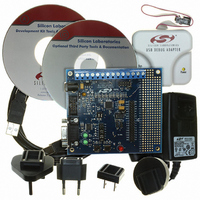
DEV KIT FOR F350/351/352/353
Manufacturer
Silicon Laboratories Inc
Type
MCUr
Specifications of C8051F350DK
Contents
Evaluation Board, Power Supply, USB Cables, Adapter and Documentation
Processor To Be Evaluated
C8051F35x
Interface Type
USB
Silicon Manufacturer
Silicon Labs
Core Architecture
8051
Silicon Core Number
C8051F350
Silicon Family Name
C8051F35x
Lead Free Status / RoHS Status
Contains lead / RoHS non-compliant
For Use With/related Products
C8051F350, 351, 352, 353
Lead Free Status / Rohs Status
Lead free / RoHS Compliant
Other names
336-1083
Available stocks
Company
Part Number
Manufacturer
Quantity
Price
Company:

Part Number:
C8051F350DK
Manufacturer:
SiliconL
Quantity:
8


C8051F350/1/2/3
50
Bit 7:
Bit 6:
Bits 5–4: RESERVED: Must Write to 00b.
Bit 3:
Bits 2–0: AD0SM: ADC0 System Mode Select.
AD0EN
R/W
Bit7
AD0EN: ADC0 Enable Bit.
0: ADC0 Disabled. ADC is in low-power shutdown.
1: ADC0 Enabled. ADC is active and ready to perform calibrations or conversions.
Note: Disabling the ADC automatically resets the AD0SM bits back to the "Idle" state.
Unused: Read = 0b, Write = don’t care.
Unused: Read = 0b, Write = don’t care.
These bits define the operating mode for the ADC. They are used to initiate all ADC conver-
sion and calibration cycles.
000: Idle
001: Full Internal Calibration (offset and gain).
010: Single Conversion.
011: Continuous Conversion.
100: Internal Offset Calibration.
101: Internal Gain Calibration.
110: System Offset Calibration.
111: System Gain Calibration.
Note: Any system mode change by the user during a conversion or calibration will
terminate the operation, and corrupt the result. To write to many of the other ADC reg-
isters, the AD0SM bits must be set to IDLE mode (000b).
Note: During an ADC conversion or calibration, the AD0SM bits may return intermedi-
ate values if they are read. It is not recommended to use these bits as indicator of the
ADC status. Only the ADC0STA register should be used as indicator of the ADC sta-
tus.
Bit6
—
R
Reserved Reserved
SFR Definition 5.3. ADC0MD: ADC0 Mode
R/W
Bit5
R/W
Bit4
Rev. 1.1
Bit3
—
R
R/W
Bit2
AD0SM
R/W
Bit1
SFR Address:
R/W
Bit0
0xF3
00000000
Reset Value
Related parts for C8051F350DK
Image
Part Number
Description
Manufacturer
Datasheet
Request
R

Part Number:
Description:
SMD/C°/SINGLE-ENDED OUTPUT SILICON OSCILLATOR
Manufacturer:
Silicon Laboratories Inc
Part Number:
Description:
Manufacturer:
Silicon Laboratories Inc
Datasheet:
Part Number:
Description:
N/A N/A/SI4010 AES KEYFOB DEMO WITH LCD RX
Manufacturer:
Silicon Laboratories Inc
Datasheet:
Part Number:
Description:
N/A N/A/SI4010 SIMPLIFIED KEY FOB DEMO WITH LED RX
Manufacturer:
Silicon Laboratories Inc
Datasheet:
Part Number:
Description:
N/A/-40 TO 85 OC/EZLINK MODULE; F930/4432 HIGH BAND (REV E/B1)
Manufacturer:
Silicon Laboratories Inc
Part Number:
Description:
EZLink Module; F930/4432 Low Band (rev e/B1)
Manufacturer:
Silicon Laboratories Inc
Part Number:
Description:
I°/4460 10 DBM RADIO TEST CARD 434 MHZ
Manufacturer:
Silicon Laboratories Inc
Part Number:
Description:
I°/4461 14 DBM RADIO TEST CARD 868 MHZ
Manufacturer:
Silicon Laboratories Inc
Part Number:
Description:
I°/4463 20 DBM RFSWITCH RADIO TEST CARD 460 MHZ
Manufacturer:
Silicon Laboratories Inc
Part Number:
Description:
I°/4463 20 DBM RADIO TEST CARD 868 MHZ
Manufacturer:
Silicon Laboratories Inc
Part Number:
Description:
I°/4463 27 DBM RADIO TEST CARD 868 MHZ
Manufacturer:
Silicon Laboratories Inc
Part Number:
Description:
I°/4463 SKYWORKS 30 DBM RADIO TEST CARD 915 MHZ
Manufacturer:
Silicon Laboratories Inc
Part Number:
Description:
N/A N/A/-40 TO 85 OC/4463 RFMD 30 DBM RADIO TEST CARD 915 MHZ
Manufacturer:
Silicon Laboratories Inc
Part Number:
Description:
I°/4463 20 DBM RADIO TEST CARD 169 MHZ
Manufacturer:
Silicon Laboratories Inc