C8051F350DK Silicon Laboratories Inc, C8051F350DK Datasheet - Page 52
C8051F350DK
Manufacturer Part Number
C8051F350DK
Description
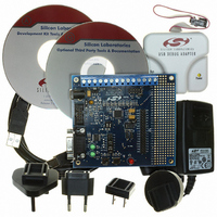
DEV KIT FOR F350/351/352/353
Manufacturer
Silicon Laboratories Inc
Type
MCUr
Specifications of C8051F350DK
Contents
Evaluation Board, Power Supply, USB Cables, Adapter and Documentation
Processor To Be Evaluated
C8051F35x
Interface Type
USB
Silicon Manufacturer
Silicon Labs
Core Architecture
8051
Silicon Core Number
C8051F350
Silicon Family Name
C8051F35x
Lead Free Status / RoHS Status
Contains lead / RoHS non-compliant
For Use With/related Products
C8051F350, 351, 352, 353
Lead Free Status / Rohs Status
Lead free / RoHS Compliant
Other names
336-1083
Available stocks
Company
Part Number
Manufacturer
Quantity
Price
Company:

Part Number:
C8051F350DK
Manufacturer:
SiliconL
Quantity:
8


C8051F350/1/2/3
52
Bits 7–0: DECI[7:0]: ADC0 Decimation Ratio Register, Bits 7–0.
This SFR can only be modified when ADC0 is in IDLE mode.
Bits 7–0: ADC0DAC: ADC0 PGA Offset DAC Magnitude.
This SFR can only be modified when ADC0 is in IDLE mode.
DECI7
SFR Definition 5.6. ADC0DECL: ADC0 Decimation Ratio Register Low Byte
R/W
R/W
Bit7
Bit7
This register contains the low byte of the 11-bit ADC Decimation Ratio. The decimation ratio
determines the number of modulator input samples used to generate a single output word
from the ADC.
The ADC0 decimation ratio is defined as:
Decimation Ratio = DECI[10:0] + 1
The corresponding sampling period and output word rate of ADC0 is:
ADC0 Conversion Period = [(DECI[10:0] + 1) * 128] / MDCLK
ADC0 Output Word Rate = MDCLK / [128 * (DECI[10:0] + 1)]
The minimum decimation ratio setting is 20. Any register setting below 19 will automatically
be interpreted as 19.
Important: When using the fast filter, the decimation ratio must be divisible by 8
(DECI[2:0] = 111b).
This register determines the ADC0 Offset DAC Magnitude. The value in the offset DAC is a
signed-magnitude representation. Bit 7 represents the sign value (0 = positive, 1 = nega-
tive), while Bits 6–0 represent the magnitude.
DECI6
R/W
R/W
Bit6
Bit6
SFR Definition 5.7. ADC0DAC: ADC0 Offset DAC
DECI5
R/W
R/W
Bit5
Bit5
DECI4
R/W
R/W
Bit4
Bit4
ADC0DAC
Rev. 1.1
DECI3
R/W
R/W
Bit3
Bit3
DECI2
R/W
R/W
Bit2
Bit2
DECI1
R/W
R/W
Bit1
Bit1
SFR Address:
SFR Address:
DECI0
R/W
R/W
Bit0
Bit0
0x9A
0xBF
00000000
Reset Value
Reset Value
11111111
Related parts for C8051F350DK
Image
Part Number
Description
Manufacturer
Datasheet
Request
R

Part Number:
Description:
SMD/C°/SINGLE-ENDED OUTPUT SILICON OSCILLATOR
Manufacturer:
Silicon Laboratories Inc
Part Number:
Description:
Manufacturer:
Silicon Laboratories Inc
Datasheet:
Part Number:
Description:
N/A N/A/SI4010 AES KEYFOB DEMO WITH LCD RX
Manufacturer:
Silicon Laboratories Inc
Datasheet:
Part Number:
Description:
N/A N/A/SI4010 SIMPLIFIED KEY FOB DEMO WITH LED RX
Manufacturer:
Silicon Laboratories Inc
Datasheet:
Part Number:
Description:
N/A/-40 TO 85 OC/EZLINK MODULE; F930/4432 HIGH BAND (REV E/B1)
Manufacturer:
Silicon Laboratories Inc
Part Number:
Description:
EZLink Module; F930/4432 Low Band (rev e/B1)
Manufacturer:
Silicon Laboratories Inc
Part Number:
Description:
I°/4460 10 DBM RADIO TEST CARD 434 MHZ
Manufacturer:
Silicon Laboratories Inc
Part Number:
Description:
I°/4461 14 DBM RADIO TEST CARD 868 MHZ
Manufacturer:
Silicon Laboratories Inc
Part Number:
Description:
I°/4463 20 DBM RFSWITCH RADIO TEST CARD 460 MHZ
Manufacturer:
Silicon Laboratories Inc
Part Number:
Description:
I°/4463 20 DBM RADIO TEST CARD 868 MHZ
Manufacturer:
Silicon Laboratories Inc
Part Number:
Description:
I°/4463 27 DBM RADIO TEST CARD 868 MHZ
Manufacturer:
Silicon Laboratories Inc
Part Number:
Description:
I°/4463 SKYWORKS 30 DBM RADIO TEST CARD 915 MHZ
Manufacturer:
Silicon Laboratories Inc
Part Number:
Description:
N/A N/A/-40 TO 85 OC/4463 RFMD 30 DBM RADIO TEST CARD 915 MHZ
Manufacturer:
Silicon Laboratories Inc
Part Number:
Description:
I°/4463 20 DBM RADIO TEST CARD 169 MHZ
Manufacturer:
Silicon Laboratories Inc