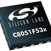
C8051F530-TB Silicon Laboratories Inc, C8051F530-TB Datasheet - Page 149

C8051F530-TB
Manufacturer Part Number
C8051F530-TB
Description
BOARD PROTOTYPE W/C8051F530
Manufacturer
Silicon Laboratories Inc
Type
MCUr
Datasheet
1.C8051F530-TB.pdf
(218 pages)
Specifications of C8051F530-TB
Contents
Board
Processor To Be Evaluated
C8051F52xA and C8051F53xA
Interface Type
USB
Lead Free Status / RoHS Status
Vendor undefined / Vendor undefined
For Use With/related Products
C8051F530
Lead Free Status / Rohs Status
Lead free / RoHS Compliant
- Current page: 149 of 218
- Download datasheet (2Mb)
SFR Definition 15.2. SBUF0: Serial (UART0) Port Data Buffer
Table 15.1. Timer Settings for Standard Baud Rates
Using the Internal Oscillator
Bits7–0: SBUF0[7:0]: Serial Data Buffer Bits 7–0 (MSB–LSB)
R/W
Bit7
Frequency: 24.5 MHz
Target
Baud Rate
(bps)
This SFR accesses two registers; a transmit shift register and a receive latch register. When
data is written to SBUF0, it goes to the transmit shift register and is held for serial transmis-
sion. Writing a byte to SBUF0 initiates the transmission. A read of SBUF0 returns the con-
tents of the receive latch.
230400
115200
57600
28800
14400
9600
2400
1200
R/W
Bit6
Baud Rate
% Error
X = Don’t care
Note: SCA1
–0.32%
–0.32%
–0.32%
–0.32%
–0.32%
0.15%
0.15%
0.15%
R/W
Bit5
–
SCA0 and T1M bit definitions can be found in Section 18.1.
Oscillator
Divide
Factor
R/W
Bit4
10176
20448
C8051F52x/F52xA/F53x/F53xA
1704
2544
106
212
426
848
Rev. 1.3
Timer Clock
Source
SYSCLK / 12
SYSCLK / 12
SYSCLK / 48
SYSCLK / 48
R/W
SYSCLK / 4
Bit3
SYSCLK
SYSCLK
SYSCLK
R/W
Bit2
SCA1–SCA0
(pre-scale
select)*
XX
XX
XX
01
00
00
10
10
R/W
Bit1
SFR Address:
T1M* Timer 1
R/W
Bit0
1
1
1
0
0
0
0
0
Reload
Value (hex)
00000000
Reset Value
0xCB
0x96
0x2B
0x96
0xB9
0x2B
0x96
0x96
0x99
149
Related parts for C8051F530-TB
Image
Part Number
Description
Manufacturer
Datasheet
Request
R
Part Number:
Description:
SMD/C°/SINGLE-ENDED OUTPUT SILICON OSCILLATOR
Manufacturer:
Silicon Laboratories Inc
Part Number:
Description:
Manufacturer:
Silicon Laboratories Inc
Datasheet:
Part Number:
Description:
N/A N/A/SI4010 AES KEYFOB DEMO WITH LCD RX
Manufacturer:
Silicon Laboratories Inc
Datasheet:
Part Number:
Description:
N/A N/A/SI4010 SIMPLIFIED KEY FOB DEMO WITH LED RX
Manufacturer:
Silicon Laboratories Inc
Datasheet:
Part Number:
Description:
N/A/-40 TO 85 OC/EZLINK MODULE; F930/4432 HIGH BAND (REV E/B1)
Manufacturer:
Silicon Laboratories Inc
Part Number:
Description:
EZLink Module; F930/4432 Low Band (rev e/B1)
Manufacturer:
Silicon Laboratories Inc
Part Number:
Description:
I°/4460 10 DBM RADIO TEST CARD 434 MHZ
Manufacturer:
Silicon Laboratories Inc
Part Number:
Description:
I°/4461 14 DBM RADIO TEST CARD 868 MHZ
Manufacturer:
Silicon Laboratories Inc
Part Number:
Description:
I°/4463 20 DBM RFSWITCH RADIO TEST CARD 460 MHZ
Manufacturer:
Silicon Laboratories Inc
Part Number:
Description:
I°/4463 20 DBM RADIO TEST CARD 868 MHZ
Manufacturer:
Silicon Laboratories Inc
Part Number:
Description:
I°/4463 27 DBM RADIO TEST CARD 868 MHZ
Manufacturer:
Silicon Laboratories Inc
Part Number:
Description:
I°/4463 SKYWORKS 30 DBM RADIO TEST CARD 915 MHZ
Manufacturer:
Silicon Laboratories Inc
Part Number:
Description:
N/A N/A/-40 TO 85 OC/4463 RFMD 30 DBM RADIO TEST CARD 915 MHZ
Manufacturer:
Silicon Laboratories Inc
Part Number:
Description:
I°/4463 20 DBM RADIO TEST CARD 169 MHZ
Manufacturer:
Silicon Laboratories Inc


