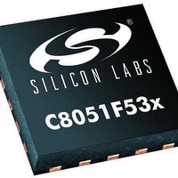
C8051F530-TB Silicon Laboratories Inc, C8051F530-TB Datasheet - Page 215

C8051F530-TB
Manufacturer Part Number
C8051F530-TB
Description
BOARD PROTOTYPE W/C8051F530
Manufacturer
Silicon Laboratories Inc
Type
MCUr
Datasheet
1.C8051F530-TB.pdf
(218 pages)
Specifications of C8051F530-TB
Contents
Board
Processor To Be Evaluated
C8051F52xA and C8051F53xA
Interface Type
USB
Lead Free Status / RoHS Status
Vendor undefined / Vendor undefined
For Use With/related Products
C8051F530
Lead Free Status / Rohs Status
Lead free / RoHS Compliant
- Current page: 215 of 218
- Download datasheet (2Mb)
D
Revision 0.3 to 0.4
Revision 0.4 to 0.5
Revision 0.5 to 1.0
Revision 1.0 to 1.1
Revision 1.1 to 1.2
Note: All items from the C8051F52xA-F53xA Errata dated August 26, 2009 are incorporated into this data sheet.
OCUMENT
Updated all specification tables.
Added 'F52xA and 'F53xA information.
Updated the Selectable Gain section in the ADC section.
Updated the External Crystal Example in the Oscillators section.
Updated the LIN section.
Updated all specification tables.
Updated Figures 1.1, 1.2, 1.3, and 1.4.
Updated Section 4 pinout diagrams and tables.
Updated all specification tables and moved them to one section.
Added Figure 3.1 and Figure 3.2.
Updated Section 4 pinout diagrams and tables.
Updated Figure 5.6.
Added Figure 15.3.
Updated equations in Section 17.
Updated Figure 21.3.
Updated Table 2.3, “ADC0 Electrical Characteristics,” on page 29 with new Burst Mode Oscillator
specification, new Power Supply Current maximum, and made corrections to Temperature Sensor
Offset and Offset Error conditions.
Updated Table 2.8, “Flash Electrical Characteristics,” on page 33 with new Flash Write and Erase
timing.
Made correction in Equivalent Gain table in Section “4.4. Selectable Gain” on page 60.
Updated Section “11.2. Power-Fail Reset / VDD Monitor” on page 107 regarding higher V
threshold.
Updated “Ordering Information” on page 14 and Table 1.1, “Product Selection Guide (Recommended
for New Designs),” on page 14 to include -A (Automotive) devices and automotive qualification
information.
Updated Table 2.3, “ADC0 Electrical Characteristics,” on page 29 to include Temperature Sensor
tracking time requirement and update INL maximum specification.
Updated Figure 3.1. ’DFN-10 Package Diagram’ on page 38 with new Pin-1 detail drawing.
Updated Table 8.1, “CIP-51 Instruction Set Summary,” on page 83 with correct CJNE and CPL timing.
Updated “Power-Fail Reset / VDD Monitor” on page 107 to clarify the recommendations for the VDD
monitor.
C
HANGE
L
IST
C8051F52x/F52xA/F53x/F53xA
Rev. 1.3
DD
monitor
215
Related parts for C8051F530-TB
Image
Part Number
Description
Manufacturer
Datasheet
Request
R
Part Number:
Description:
SMD/C°/SINGLE-ENDED OUTPUT SILICON OSCILLATOR
Manufacturer:
Silicon Laboratories Inc
Part Number:
Description:
Manufacturer:
Silicon Laboratories Inc
Datasheet:
Part Number:
Description:
N/A N/A/SI4010 AES KEYFOB DEMO WITH LCD RX
Manufacturer:
Silicon Laboratories Inc
Datasheet:
Part Number:
Description:
N/A N/A/SI4010 SIMPLIFIED KEY FOB DEMO WITH LED RX
Manufacturer:
Silicon Laboratories Inc
Datasheet:
Part Number:
Description:
N/A/-40 TO 85 OC/EZLINK MODULE; F930/4432 HIGH BAND (REV E/B1)
Manufacturer:
Silicon Laboratories Inc
Part Number:
Description:
EZLink Module; F930/4432 Low Band (rev e/B1)
Manufacturer:
Silicon Laboratories Inc
Part Number:
Description:
I°/4460 10 DBM RADIO TEST CARD 434 MHZ
Manufacturer:
Silicon Laboratories Inc
Part Number:
Description:
I°/4461 14 DBM RADIO TEST CARD 868 MHZ
Manufacturer:
Silicon Laboratories Inc
Part Number:
Description:
I°/4463 20 DBM RFSWITCH RADIO TEST CARD 460 MHZ
Manufacturer:
Silicon Laboratories Inc
Part Number:
Description:
I°/4463 20 DBM RADIO TEST CARD 868 MHZ
Manufacturer:
Silicon Laboratories Inc
Part Number:
Description:
I°/4463 27 DBM RADIO TEST CARD 868 MHZ
Manufacturer:
Silicon Laboratories Inc
Part Number:
Description:
I°/4463 SKYWORKS 30 DBM RADIO TEST CARD 915 MHZ
Manufacturer:
Silicon Laboratories Inc
Part Number:
Description:
N/A N/A/-40 TO 85 OC/4463 RFMD 30 DBM RADIO TEST CARD 915 MHZ
Manufacturer:
Silicon Laboratories Inc
Part Number:
Description:
I°/4463 20 DBM RADIO TEST CARD 169 MHZ
Manufacturer:
Silicon Laboratories Inc


