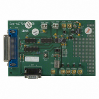
EVAL-AD7706EB Analog Devices Inc, EVAL-AD7706EB Datasheet - Page 16
EVAL-AD7706EB
Manufacturer Part Number
EVAL-AD7706EB
Description
BOARD EVAL FOR AD7706
Manufacturer
Analog Devices Inc
Datasheet
1.EVAL-AD7705EB.pdf
(32 pages)
Specifications of EVAL-AD7706EB
Number Of Adc's
1
Number Of Bits
16
Sampling Rate (per Second)
500
Data Interface
Serial
Inputs Per Adc
3 Differential
Input Range
0 ~ 5.25 V
Power (typ) @ Conditions
6.5mW @ 500SPS
Voltage Supply Source
Single
Operating Temperature
-40°C ~ 85°C
Utilized Ic / Part
AD7706
Lead Free Status / RoHS Status
Contains lead / RoHS non-compliant


AD7705/AD7706
ANALOG INPUT
Analog Input Ranges
The AD7705 contains two differential analog input pairs
AIN1(+), AIN1(–) and AIN2(+), AIN2(–). These input pairs
provide programmable-gain, differential input channels that
can handle either unipolar or bipolar input signals. It should be
noted that the bipolar input signals are referenced to the re-
spective AIN(–) input of each input pair. The AD7706 contains
three pseudo differential analog input pairs AIN1, AIN2 and
AIN3, which are referenced to the COMMON input on the part.
In unbuffered mode, the common-mode range of the input is
from GND to V
analog input voltage lies between GND – 30 mV and V
+ 30 mV. This means that in unbuffered mode the part can
handle both unipolar and bipolar input ranges for all gains.
Absolute voltages of GND – 200 mV can be accommodated on
the analog inputs at 25 C without degradation in performance,
but leakage current increases appreciably with increasing tem-
perature. In buffered mode, the analog inputs can handle
much larger source impedances, but the absolute input voltage
range is restricted to between GND + 50 mV to V
which also places restrictions on the common-mode range. This
means that in buffered mode there are some restrictions on the
allowable gains for bipolar input ranges. Care must be taken in
setting up the common-mode voltage and input voltage range
so that the above limits are not exceeded, otherwise there will
be a degradation in linearity performance.
In unbuffered mode, the analog inputs look directly into the
7 pF input sampling capacitor, C
current in this unbuffered mode is 1 nA maximum. As a result,
the analog inputs see a dynamic load that is switched at the
input sample rate (see Figure 11). This sample rate depends on
master clock frequency and selected gain. C
AIN(+) and discharged to AIN(–) every input sample cycle.
The effective on-resistance of the switch, R
C
source impedances every input sample cycle. Therefore, in
unbuffered mode, source impedances mean a longer charge time
for C
XIV shows the allowable external resistance/capacitance values,
for unbuffered mode, such that no gain error to the 16-bit level
is introduced on the part. Note that these capacitances are
total capacitances on the analog input, external capacitance
plus 10 pF capacitance from the pins and lead frame of the device.
SAMP
SAMP
Figure 11. Unbuffered Analog Input Structure
must be charged through R
AIN(+)
AIN(–)
and this may result in gain errors on the part. Table
SWITCHING FREQUENCY DEPENDS ON
f
DD
CLKIN
, provided that the absolute value of the
AND SELECTED GAIN
R
SW
(7k
C
(7pF)
SAMP
TYP)
V
SAMP
BIAS
SW
and through any external
. The dc input leakage
HIGH
IMPEDANCE
SW
1G
SAMP
, is typically 7 k .
is charged to
DD
– 1.5 V
DD
–16–
Gain
1
2
4
8–128 35.2 k
In buffered mode, the analog inputs look into the high-impedance
inputs stage of the on-chip buffer amplifier. C
via this buffer amplifier such that source impedances do not
affect the charging of C
leakage current of 1 nA. In this buffered mode, large source
impedances result in a small dc offset voltage developed across
the source impedance, but not in a gain error.
Input Sample Rate
The modulator sample frequency for the AD7705/AD7706
remains at f
gardless of the selected gain. However, gains greater than 1 are
achieved by a combination of multiple input samples per modu-
lator cycle and a scaling of the ratio of reference capacitor to
input capacitor. As a result of the multiple sampling, the input
sample rate of the device varies with the selected gain (see Table
XV). In buffered mode, the input is buffered before the input
sampling capacitor. In unbuffered mode, where the analog
input looks directly into the sampling capacitor, the effective
input impedance is 1/C
pling capacitance and f
Gain
1
2
4
8–128
Bipolar/Unipolar Inputs
The analog inputs on the AD7705/AD7706 can accept either
unipolar or bipolar input voltage ranges. Bipolar input ranges do
not imply that the part can handle negative voltages on its analog
input, since the analog input cannot go more negative than
–30 mV to ensure correct operation of these parts. The input
channels are fully differential. As a result, on the AD7705, the
voltage to which the unipolar and bipolar signals on the AIN(+)
input are referenced is the voltage on the respective AIN(–)
input. On the AD7706, the voltages applied to the analog input
channels are referenced to the COMMON input. For example, if
AIN1(–) is +2.5 V and the AD7705 is configured for unipolar
operation with a gain of 2 and a V
range on the AIN1(+) input is +2.5 V to +3.75 V. If AIN1(–) is
+2.5 V and the AD7705 is configured for bipolar mode with a
gain of 2 and a V
AIN1(+) input is +1.25 V to +3.75 V (i.e., 2.5 V
AIN1(–) is at GND, the part cannot be configured for bipolar
ranges in excess of 30 mV.
Table XIV. External R, C Combination for No 16-Bit Gain
Error (Unbuffered Mode Only)
0
368 k
177.2 k
82.8 k
Table XV. Input Sampling Frequency vs. Gain
f
2
4
8
CLKIN
Input Sampling Frequency (f
CLKIN
f
f
f
CLKIN
CLKIN
CLKIN
/128 (19.2 kHz @ f
REF
/64 (38.4 kHz @ f
50
90.6 k
44.2 k
21.2 k
9.6 k
of +2.5 V, the analog input range on the
/64 (76.8 kHz @ f
/64 (76.8 kHz @ f
/64 (307.2 kHz @ f
S
SAMP
SAMP
External Capacitance (pF)
is the input sample rate.
. This buffer amplifier has an offset
100
54.2 k
26.4 k
12.6 k
5.8 k
f
S
where C
REF
CLKIN
CLKIN
of +2.5 V, the input voltage
500
14.6 k
7.2 k
CLKIN
CLKIN
3.4 k
1.58
CLKIN
SAMP
= 2.4576 MHz)
= 2.4576 MHz) re-
S
)
= 2.4576 MHz)
= 2.4576 MHz)
is the input sam-
= 2.4576 MHz)
SAMP
1000
8.2 k
4 k
1.94 k
880
1.25 V). If
is charged
REV. A
5000
2.2 k
1.12 k
540
240
Related parts for EVAL-AD7706EB
Image
Part Number
Description
Manufacturer
Datasheet
Request
R

Part Number:
Description:
ENERCHIP CC EVAL KIT
Manufacturer:
Cymbet Corporation
Datasheet:

Part Number:
Description:
BOARD EVAL FOR AD976
Manufacturer:
Analog Devices Inc
Datasheet:

Part Number:
Description:
BOARD EVAL FOR ADXL345
Manufacturer:
Analog Devices Inc
Datasheet:

Part Number:
Description:
ENERCHIP CC SEH EVAL KIT
Manufacturer:
Cymbet Corporation
Datasheet:

Part Number:
Description:
ENERCHIP EP ENERGY HARVEST EVAL
Manufacturer:
Cymbet Corporation
Datasheet:

Part Number:
Description:
EVAL BOARD FOR TW6864-LB2-GR
Manufacturer:
Intersil
Datasheet:
Part Number:
Description:
EVAL BOARD FOR TW8816-LB3-GR
Manufacturer:
Intersil
Datasheet:
Part Number:
Description:
EVAL BOARD FOR TW8817-TA3-GRS
Manufacturer:
Intersil
Datasheet:

Part Number:
Description:
EVALUATION MODULE FOR ADUM4160
Manufacturer:
Analog Devices Inc
Datasheet:

Part Number:
Description:
BOARD EVALUATION ADCMP581BCP
Manufacturer:
Analog Devices Inc
Datasheet:
Part Number:
Description:
BOARD EVALUATION ADM1041
Manufacturer:
Analog Devices Inc
Datasheet:

Part Number:
Description:
EVAL BOARD FOR STM32F107VCT
Manufacturer:
STMicroelectronics
Datasheet:
Part Number:
Description:
BOARD EVAL FOR AD1954
Manufacturer:
Analog Devices Inc
Datasheet:
Part Number:
Description:
BOARD EVAL FOR AD1955
Manufacturer:
Analog Devices Inc
Datasheet:

Part Number:
Description:
BOARD EVAL FOR AD7655
Manufacturer:
Analog Devices Inc
Datasheet: