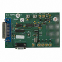
EVAL-AD7706EB Analog Devices Inc, EVAL-AD7706EB Datasheet - Page 3
EVAL-AD7706EB
Manufacturer Part Number
EVAL-AD7706EB
Description
BOARD EVAL FOR AD7706
Manufacturer
Analog Devices Inc
Datasheet
1.EVAL-AD7705EB.pdf
(32 pages)
Specifications of EVAL-AD7706EB
Number Of Adc's
1
Number Of Bits
16
Sampling Rate (per Second)
500
Data Interface
Serial
Inputs Per Adc
3 Differential
Input Range
0 ~ 5.25 V
Power (typ) @ Conditions
6.5mW @ 500SPS
Voltage Supply Source
Single
Operating Temperature
-40°C ~ 85°C
Utilized Ic / Part
AD7706
Lead Free Status / RoHS Status
Contains lead / RoHS non-compliant


REV. A
Parameter
LOGIC OUTPUTS (Including MCLK OUT)
SYSTEM CALIBRATION
POWER REQUIREMENTS
NOTES
10
11
12
13
14
15
16
17
18
19
Specifications subject to change without notice.
1
2
3
4
5
6
7
8
9
Temperature range as follows: B Version, –40 C to +85 C.
These numbers are established from characterization or design at initial product release.
A calibration is effectively a conversion so these errors will be of the order of the conversion noise shown in Tables I and III. This applies after calibration at the
Recalibration at any temperature will remove these drift errors.
Positive Full-Scale Error includes Zero-Scale Errors (Unipolar Offset Error or Bipolar Zero Error) and applies to both unipolar and bipolar input ranges.
Full-Scale Drift includes Zero-Scale Drift (Unipolar Offset Drift or Bipolar Zero Drift) and applies to both unipolar and bipolar input ranges.
Gain Error does not include Zero-Scale Errors. It is calculated as Full-Scale Error–Unipolar Offset Error for unipolar ranges and Full-Scale Error–Bipolar Zero Error for
Gain Error Drift does not include Unipolar Offset Drift/Bipolar Zero Drift. It is effectively the drift of the part if zero scale calibrations only were performed.
This common-mode voltage range is allowed provided that the input voltage on analog inputs does not go more positive than V
The analog input voltage range on AIN(+) is given here with respect to the voltage on AIN(–) on the AD7705 and is given with respect to the COMMON input on the
V
These logic output levels apply to the MCLK OUT only when it is loaded with one CMOS load.
Sample tested at +25 C to ensure compliance.
After calibration, if the analog input exceeds positive full scale, the converter will output all 1s. If the analog input is less than negative full scale, the device will output all 0s.
These calibration and span limits apply provided the absolute voltage on the analog inputs does not exceed V
When using a crystal or ceramic resonator across the MCLK pins as the clock source for the device, the V
If the external master clock continues to run in standby mode, the standby current increases to 150 A typical at 5 V and 75 A at 3 V. When using a crystal or ceramic
Measured at dc and applies in the selected passband. PSRR at 50 Hz will exceed 120 dB with filter notches of 25 Hz or 50 Hz. PSRR at 60 Hz will exceed 120 dB with filter
PS
temperature of interest.
bipolar ranges.
GND – 30 mV. Parts are functional with voltages down to GND – 200 mV, but with increased leakage at high temperature.
AD7706. The absolute voltage on the analog inputs should not go more positive than V
voltages of GND – 200 mV can be accommodated, but with increased leakage at high temperature.
calibration limit applies to both the unipolar zero point and the bipolar zero point.
resonator type (see Clocking and Oscillator Circuit section).
resonator across the MCLK pins as the clock source for the device, the internal oscillator continues to run in standby mode and the power dissipation depends on the crystal
or resonator type (see Standby Mode section).
notches of 20 Hz or 60 Hz.
Gain
V
V
V
V
V
V
Floating State Leakage Current
Floating State Output Capacitance
Data Output Coding
Positive Full-Scale Calibration Limit
Negative Full-Scale Calibration Limit
Offset Calibration Limit
Input Span
V
V
Standby (Power-Down) Current
Power Supply Rejection
REF
DD
DD
RR depends on both gain and V
OL
OL
OH
OH
DD
DD
Power Supply Currents
Power Supply Currents
= REF IN(+) – REF IN(–).
= 3 V
= 5 V
, Output Low Voltage
, Output Low Voltage
, Output High Voltage
, Output High Voltage
Voltage
Voltage
15
1
86
90
2
78
78
18
14
16
16
4
85
84
DD
17
8–128
93
91
.
13
14
14
B Version
0.4
0.4
4
V
9
Binary
Offset Binary
(1.05
–(1.05
–(1.05
(0.8
(2.1
+2.7 to +3.3
0.32
0.6
0.4
0.6
0.7
1.1
+4.75 to +5.25
0.45
0.7
0.6
0.85
0.9
1.3
16
8
See Note 19
10
DD
–0.6
V
V
V
REF
REF
V
V
REF
1
REF
REF
)/GAIN
)/GAIN
)/GAIN
)/GAIN
)/GAIN
Units
V max
V max
V min
V min
pF typ
V max
V max
V max
V min
V max
V min to V max
mA max
mA max
mA max
mA max
mA max
mA max
V min to V max
mA max
mA max
mA max
mA max
mA max
mA max
dB typ
–3–
A max
A max
A max
DD
+ 30 mV, or go more negative than GND – 30 mV for specified performance, input
DD
DD
current and power dissipation will vary depending on the crystal or
Conditions/Comments
I
I
I
I
Unipolar Mode
Bipolar Mode
GAIN Is the Selected PGA Gain (1 to 128)
GAIN Is the Selected PGA Gain (1 to 128)
GAIN Is the Selected PGA Gain (1 to 128)
GAIN Is the Selected PGA Gain (1 to 128)
GAIN Is the Selected PGA Gain (1 to 128)
For Specified Performance
Digital I/Ps = 0 V or V
CLK DIS = 1
BUF Bit = 0. f
BUF Bit = 1. f
BUF Bit = 0. f
BUF Bit = 0. f
BUF Bit = 1. f
BUF Bit = 1. f
For Specified Performance
Digital I/Ps = 0 V or V
CLK DIS = 1.
BUF Bit = 0. f
BUF Bit = 1. f
BUF Bit = 0. f
BUF Bit = 0. f
BUF Bit = 1. f
BUF Bit = 1. f
External MCLK IN = 0 V or V
External MCLK IN = 0 V or V
SINK
SINK
SOURCE
SOURCE
+ 30 mV or go more negative than GND – 30 mV. The offset
= 800 A Except for MCLK OUT.
= 100 A Except for MCLK OUT.
= 200 A Except for MCLK OUT.
= 100 A Except for MCLK OUT.
CLKIN
CLKIN
CLKIN
CLKIN
CLKIN
CLKIN
CLKIN
CLKIN
CLKIN
CLKIN
CLKIN
CLKIN
DD
+ 30 mV or go more negative than
= 1 MHz. Gains of 1 to 128
= 1 MHz. Gains of 1 to 128
= 2.4576 MHz. Gains of 1 to 4
= 2.4576 MHz. Gains of 8 to 128
= 2.4576 MHz. Gains of 1 to 4
= 2.4576 MHz. Gains of 8 to 128
= 1 MHz. Gains of 1 to 128
= 1 MHz. Gains of 1 to 128
= 2.4576 MHz. Gains of 1 to 4
= 2.4576 MHz. Gains of 8 to 128
= 2.4576 MHz. Gains of 1 to 4
= 2.4576 MHz. Gains of 8 to 128
DD
DD
. External MCLK IN and
. External MCLK IN and
AD7705/AD7706
DD
DD
. V
. V
DD
DD
= 5 V. See Figure 9
= 3 V
12
12
V
V
12
12
DD
DD
V
V
DD
DD
= 5 V.
= 3 V.
= 5 V.
= 3 V.
Related parts for EVAL-AD7706EB
Image
Part Number
Description
Manufacturer
Datasheet
Request
R

Part Number:
Description:
ENERCHIP CC EVAL KIT
Manufacturer:
Cymbet Corporation
Datasheet:

Part Number:
Description:
BOARD EVAL FOR AD976
Manufacturer:
Analog Devices Inc
Datasheet:

Part Number:
Description:
BOARD EVAL FOR ADXL345
Manufacturer:
Analog Devices Inc
Datasheet:

Part Number:
Description:
ENERCHIP CC SEH EVAL KIT
Manufacturer:
Cymbet Corporation
Datasheet:

Part Number:
Description:
ENERCHIP EP ENERGY HARVEST EVAL
Manufacturer:
Cymbet Corporation
Datasheet:

Part Number:
Description:
EVAL BOARD FOR TW6864-LB2-GR
Manufacturer:
Intersil
Datasheet:
Part Number:
Description:
EVAL BOARD FOR TW8816-LB3-GR
Manufacturer:
Intersil
Datasheet:
Part Number:
Description:
EVAL BOARD FOR TW8817-TA3-GRS
Manufacturer:
Intersil
Datasheet:

Part Number:
Description:
EVALUATION MODULE FOR ADUM4160
Manufacturer:
Analog Devices Inc
Datasheet:

Part Number:
Description:
BOARD EVALUATION ADCMP581BCP
Manufacturer:
Analog Devices Inc
Datasheet:
Part Number:
Description:
BOARD EVALUATION ADM1041
Manufacturer:
Analog Devices Inc
Datasheet:

Part Number:
Description:
EVAL BOARD FOR STM32F107VCT
Manufacturer:
STMicroelectronics
Datasheet:
Part Number:
Description:
BOARD EVAL FOR AD1954
Manufacturer:
Analog Devices Inc
Datasheet:
Part Number:
Description:
BOARD EVAL FOR AD1955
Manufacturer:
Analog Devices Inc
Datasheet:

Part Number:
Description:
BOARD EVAL FOR AD7655
Manufacturer:
Analog Devices Inc
Datasheet: