EVAL-AD7706EB Analog Devices Inc, EVAL-AD7706EB Datasheet - Page 7
EVAL-AD7706EB
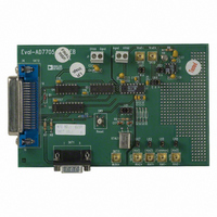
Manufacturer Part Number
EVAL-AD7706EB
Description
BOARD EVAL FOR AD7706
Manufacturer
Analog Devices Inc
Datasheet
1.EVAL-AD7705EB.pdf
(32 pages)
Specifications of EVAL-AD7706EB
Number Of Adc's
1
Number Of Bits
16
Sampling Rate (per Second)
500
Data Interface
Serial
Inputs Per Adc
3 Differential
Input Range
0 ~ 5.25 V
Power (typ) @ Conditions
6.5mW @ 500SPS
Voltage Supply Source
Single
Operating Temperature
-40°C ~ 85°C
Utilized Ic / Part
AD7706
Lead Free Status / RoHS Status
Contains lead / RoHS non-compliant


REV. A
Pin No.
10
11
12
13
14
15
16
OUTPUT NOISE (5 V OPERATION)
Table I shows the AD7705/AD7706 output rms noise for the selectable notch and –3 dB frequencies for the part, as selected by FS0
and FS1 of the Clock Register. The numbers given are for the bipolar input ranges with a V
numbers are typical and are generated at an analog input voltage of 0 V with the part used in either buffered or unbuffered mode. Table II
meanwhile shows the output peak-to-peak noise for the selectable notch and –3 dB frequencies for the part. It is important to note that
these numbers represent the resolution for which there will be no code flicker. They are not calculated based on rms noise but on peak-to-peak
noise. The numbers given are for bipolar input ranges with a V
bers are typical and are rounded to the nearest LSB. The numbers apply for the CLK DIV bit of the Clock Register set to 0.
Filter First
Notch and O/P –3 dB
Data Rate
MCLK IN = 2.4576 MHz
50 Hz
60 Hz
250 Hz
500 Hz
MCLK IN = 1 MHz
20 Hz
25 Hz
100 Hz
200 Hz
Mnemonic
REF IN(–)
AIN2(–)[AIN3]
DRDY
DOUT
DIN
V
GND
DD
Frequency
13.1 Hz
15.72 Hz
65.5 Hz
131 Hz
5.24 Hz
6.55 Hz
26.2 Hz
52.4 Hz
Table I. Output RMS Noise vs. Gain and Output Update Rate @ 5 V
Gain of
1
4.1
5.1
110
550
4.1
5.1
110
550
Function
Reference Input. Negative input of the differential reference input to the AD7705/AD7706.
The REF IN(–) can lie anywhere between V
than REF IN(–).
AD7705: Negative input of the differential analog Input Channel 2. AD7706: Analog Input
Channel 3.
Logic Output. A logic low on this output indicates that a new output word is available from
the AD7705/AD7706 data register. The DRDY pin will return high upon completion of a
read operation of a full output word. If no data read has taken place between output updates,
the DRDY line will return high for 500
While DRDY is high, a read operation should neither be attempted nor in progress to avoid
reading from the data register as it is being updated. The DRDY line will return low again
when the update has taken place. DRDY is also used to indicate when the AD7705/AD7706
has completed its on-chip calibration sequence.
Serial Data Output with serial data being read from the output shift register on the part. This
output shift register can contain information from the setup register, communications regis-
ter, clock register or data register, depending on the register selection bits of the Communica-
tions Register.
Serial Data Input with serial data being written to the input shift register on the part. Data
from this input shift register is transferred to the setup register, clock register or communica-
tions register, depending, on the register selection bits of the Communications Register.
Supply Voltage, +2.7 V to +5.25 V operation.
Ground reference point for the AD7705/AD7706’s internal circuitry.
Gain of
2
2.1
2.5
49
285
2.1
2.5
49
285
Typical Output RMS Noise in V
Gain of
4
1.2
1.4
31
145
1.2
1.4
31
145
REF
–7–
of +2.5 V and for either buffered or unbuffered mode. These num-
Gain of
8
0.75
0.8
17
70
0.75
0.8
17
70
t
DD
CLK IN
Gain of
16
0.7
0.75
8
41
0.7
0.75
8
41
and GND provided REF IN(+) is greater
cycles prior to the next output update.
REF
of +2.5 V and V
Gain of
32
0.66
0.7
3.6
22
0.66
0.7
3.6
22
AD7705/AD7706
Gain of
64
0.63
0.67
2.3
9.1
0.63
0.67
2.3
9.1
DD
= 5 V. These
Gain of
128
0.6
0.62
1.7
4.7
0.6
0.62
1.7
4.7
Related parts for EVAL-AD7706EB
Image
Part Number
Description
Manufacturer
Datasheet
Request
R

Part Number:
Description:
ENERCHIP CC EVAL KIT
Manufacturer:
Cymbet Corporation
Datasheet:

Part Number:
Description:
BOARD EVAL FOR AD976
Manufacturer:
Analog Devices Inc
Datasheet:

Part Number:
Description:
BOARD EVAL FOR ADXL345
Manufacturer:
Analog Devices Inc
Datasheet:

Part Number:
Description:
ENERCHIP CC SEH EVAL KIT
Manufacturer:
Cymbet Corporation
Datasheet:

Part Number:
Description:
ENERCHIP EP ENERGY HARVEST EVAL
Manufacturer:
Cymbet Corporation
Datasheet:

Part Number:
Description:
EVAL BOARD FOR TW6864-LB2-GR
Manufacturer:
Intersil
Datasheet:
Part Number:
Description:
EVAL BOARD FOR TW8816-LB3-GR
Manufacturer:
Intersil
Datasheet:
Part Number:
Description:
EVAL BOARD FOR TW8817-TA3-GRS
Manufacturer:
Intersil
Datasheet:

Part Number:
Description:
EVALUATION MODULE FOR ADUM4160
Manufacturer:
Analog Devices Inc
Datasheet:

Part Number:
Description:
BOARD EVALUATION ADCMP581BCP
Manufacturer:
Analog Devices Inc
Datasheet:
Part Number:
Description:
BOARD EVALUATION ADM1041
Manufacturer:
Analog Devices Inc
Datasheet:

Part Number:
Description:
EVAL BOARD FOR STM32F107VCT
Manufacturer:
STMicroelectronics
Datasheet:
Part Number:
Description:
BOARD EVAL FOR AD1954
Manufacturer:
Analog Devices Inc
Datasheet:
Part Number:
Description:
BOARD EVAL FOR AD1955
Manufacturer:
Analog Devices Inc
Datasheet:

Part Number:
Description:
BOARD EVAL FOR AD7655
Manufacturer:
Analog Devices Inc
Datasheet: