EVAL-AD7706EB Analog Devices Inc, EVAL-AD7706EB Datasheet - Page 23
EVAL-AD7706EB
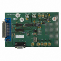
Manufacturer Part Number
EVAL-AD7706EB
Description
BOARD EVAL FOR AD7706
Manufacturer
Analog Devices Inc
Datasheet
1.EVAL-AD7705EB.pdf
(32 pages)
Specifications of EVAL-AD7706EB
Number Of Adc's
1
Number Of Bits
16
Sampling Rate (per Second)
500
Data Interface
Serial
Inputs Per Adc
3 Differential
Input Range
0 ~ 5.25 V
Power (typ) @ Conditions
6.5mW @ 500SPS
Voltage Supply Source
Single
Operating Temperature
-40°C ~ 85°C
Utilized Ic / Part
AD7706
Lead Free Status / RoHS Status
Contains lead / RoHS non-compliant


The printed circuit board that houses the AD7705 should be
designed so that the analog and digital sections are separated
and confined to certain areas of the board. This facilitates the
use of ground planes which can be separated easily. A minimum
etch technique is generally best for ground planes as it gives the
best shielding. Digital and analog ground planes should only be
joined in one place to avoid ground loops. If the AD7705/AD7706
is in a system where multiple devices require AGND-to-DGND
connections, the connection should be made at one point only,
a star ground point which should be established as close as
possible to the AD7705 GND.
Avoid running digital lines under the device as these will couple
noise onto the die. The analog ground plane should be allowed
to run under the AD7705/AD7706 to avoid noise coupling. The
power supply lines to the AD7705/AD7706 should use as large
a trace as possible to provide low impedance paths and reduce
the effects of glitches on the power supply line. Fast switching
signals like clocks should be shielded with digital ground to
avoid radiating noise to other sections of the board and clock
signals should never be run near the analog inputs. Avoid cross-
over of digital and analog signals. Traces on opposite sides of
the board should run at right angles to each other. This will
reduce the effects of feedthrough through the board. A micro-
strip technique is by far the best, but is not always possible with
a double-sided board. In this technique, the component side of
the board is dedicated to ground planes while signals are placed
on the solder side.
Good decoupling is important when using high resolution
ADCs. All analog supplies should be decoupled with 10 F
tantalum in parallel with 0.1 F ceramic capacitors to GND. To
achieve the best from these decoupling components, they have
to be placed as close as possible to the device, ideally right up
against the device. All logic chips should be decoupled with
0.1 F disc ceramic capacitors to DGND.
Evaluating the AD7705/AD7706 Performance
The recommended layout for the AD7705 and AD7706 is out-
lined in their associated evaluation. These evaluation board
packages include a fully assembled and tested evaluation board,
documentation, software for controlling the board over the
printer port of a PC and software for analyzing their perfor-
mance on the PC.
Noise levels in the signals applied to the AD7705/AD7706 may
also affect performance of the part. The AD7705/AD7706 soft-
ware evaluation package allows the user to evaluate the true
REV. A
–23–
performance of the part, independent of the analog input signal.
The scheme involves using a test mode on the part where the
inputs to the AD7705 are internally shorted together to provide
a zero differential voltage for the analog modulator. External to
the device, the AIN1(–) input on the AD7705 should be con-
nected to a voltage that is within the allowable common-mode
range of the part. Similarly, on the AD7706 the COMMON
input should be connected to a voltage within its allowable
common-mode range for evaluation purposes. This scheme should
be used after a calibration has been performed on the part.
DIGITAL INTERFACE
As previously outlined, the AD7705/AD7706’s programmable
functions are controlled using a set of on-chip registers. Data is
written to these registers via the part’s serial interface and read
access to the on-chip registers is also provided by this interface.
All communications to the part must start with a write operation
to the Communications Register. After power-on or RESET,
the device expects a write to its Communications Register. The
data written to this register determines whether the next opera-
tion to the part is a read or a write operation and also deter-
mines to which register this read or write operation occurs.
Therefore, write access to any of the other registers on the part
starts with a write operation to the Communications Register
followed by a write to the selected register. A read operation
from any other register on the part (including the output data
register) starts with a write operation to the Communications
Register followed by a read operation from the selected register.
The AD7705/AD7706’s serial interface consists of five signals,
CS, SCLK, DIN, DOUT and DRDY. The DIN line is used for
transferring data into the on-chip registers while the DOUT line
is used for accessing data from the on-chip registers. SCLK is
the serial clock input for the device and all data transfers (either
on DIN or DOUT) take place with respect to this SCLK signal.
The DRDY line is used as a status signal to indicate when data
is ready to be read from the AD7705/AD7706’s data register.
DRDY goes low when a new data word is available in the out-
put register. It is reset high when a read operation from the data
register is complete. It also goes high prior to the updating of
the output register to indicate when not to read from the device
to ensure that a data read is not attempted while the register is
being updated. CS is used to select the device. It can be used to
decode the AD7705/AD7706 in systems where a number of
parts are connected to the serial bus.
AD7705/AD7706
Related parts for EVAL-AD7706EB
Image
Part Number
Description
Manufacturer
Datasheet
Request
R

Part Number:
Description:
ENERCHIP CC EVAL KIT
Manufacturer:
Cymbet Corporation
Datasheet:

Part Number:
Description:
BOARD EVAL FOR AD976
Manufacturer:
Analog Devices Inc
Datasheet:

Part Number:
Description:
BOARD EVAL FOR ADXL345
Manufacturer:
Analog Devices Inc
Datasheet:

Part Number:
Description:
ENERCHIP CC SEH EVAL KIT
Manufacturer:
Cymbet Corporation
Datasheet:

Part Number:
Description:
ENERCHIP EP ENERGY HARVEST EVAL
Manufacturer:
Cymbet Corporation
Datasheet:

Part Number:
Description:
EVAL BOARD FOR TW6864-LB2-GR
Manufacturer:
Intersil
Datasheet:
Part Number:
Description:
EVAL BOARD FOR TW8816-LB3-GR
Manufacturer:
Intersil
Datasheet:
Part Number:
Description:
EVAL BOARD FOR TW8817-TA3-GRS
Manufacturer:
Intersil
Datasheet:

Part Number:
Description:
EVALUATION MODULE FOR ADUM4160
Manufacturer:
Analog Devices Inc
Datasheet:

Part Number:
Description:
BOARD EVALUATION ADCMP581BCP
Manufacturer:
Analog Devices Inc
Datasheet:
Part Number:
Description:
BOARD EVALUATION ADM1041
Manufacturer:
Analog Devices Inc
Datasheet:

Part Number:
Description:
EVAL BOARD FOR STM32F107VCT
Manufacturer:
STMicroelectronics
Datasheet:
Part Number:
Description:
BOARD EVAL FOR AD1954
Manufacturer:
Analog Devices Inc
Datasheet:
Part Number:
Description:
BOARD EVAL FOR AD1955
Manufacturer:
Analog Devices Inc
Datasheet:

Part Number:
Description:
BOARD EVAL FOR AD7655
Manufacturer:
Analog Devices Inc
Datasheet: